


PROBLEM?
+86 13430584894
luojunjie@piezoman.com
PAYMENT_METHOD


 AD_MSG
POP_UP_MESSAGE_CONTENT


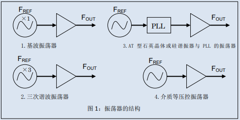
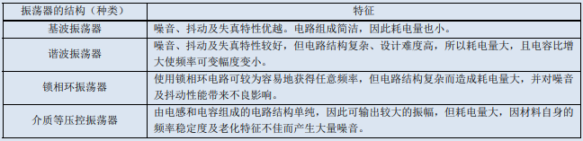
Table 1: Structure and Characteristics of Oscillators
As shown in the feature bar, the different structures of oscillators result in different characteristics. This article provides a detailed explanation of the phase noise characteristics and tendencies of fundamental oscillators, phase-locked loop oscillators, and medium voltage controlled oscillators from the perspective of noise and jitter that greatly affect the signal quality of communication systems.
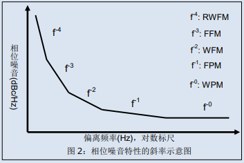
[Characteristics of Phase Noise Slope]
The phase noise exhibits the slope characteristics shown in Figure 2. This slope is divided into five categories, each with the following characteristics, which will be briefly explained here.
1) The slope of random walk frequency modulation (RWFM) noise is inversely proportional to the fourth power of the offset frequency, mainly indicating the impact of frequency changes (phase changes converted into frequency changes) of the wave source.
2) The slope of flicker frequency modulation (FFM) white noise is inversely proportional to the third power of the offset frequency, mainly indicating the influence of flicker noise from the wave source.
3) The slope of White Frequency Modulation (WFM) noise is inversely proportional to the square of the offset frequency, mainly indicating the influence of the Q-value on the circuit side.
4) The slope of Flicker Phase Modulation (FPM) noise is inversely proportional to the offset frequency, and like flicker noise, it represents the influence of noise from the oscillating side (circuit side).
5) The slope of white phase modulation (WPM) noise remains constant and independent of offset frequency, mainly representing thermal noise from circuit components) and the influence of the S/N ratio of oscillation signals.
As mentioned above, the slope of phase noise characteristics can be divided into two categories: RWFM and FFM noise affected by wave sources; WFM, FPM, and WPM noise are affected by the circuit.
[Method for calculating phase jitter based on phase noise characteristics]
In the previously published technical specification "Jitter and Phase Noise", it was also introduced that phase jitter can be calculated by integrating the specific offset frequency range of the phase noise characteristics. The performance of communication systems depends on the phase jitter in the communication loop bandwidth. Nowadays, the 12k-20MHz phase jitter in the communication loop bandwidth of many communication systems (according to the standard of SONET/SDH) has been regarded as one of the important indicators of phase jitter.
Figure 3 shows the relationship between phase noise characteristics and phase jitter.
The total jitter TJ is represented by the sum of deterministic jitter DJ and random jitter RJ. In a system with phase noise characteristics similar to those shown in Figure 3, the total amount of phase jitter is equivalent to the sum of the integrated value (RJ) of the 12k-20MHz portion (gray blue portion in Figure 3) and the integrated value (DJ) of distortion in the communication loop bandwidth.
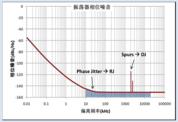
Figure 3: Relationship between phase noise and phase jitter
[Different phase noise characteristics caused by oscillator structure]
In order to help understand the differences in phase noise characteristics caused by oscillator structures, based on the structure introduced in Figure 1, the phase noise characteristics of three oscillators will be explained. These three oscillators are the fundamental oscillator with quartz crystal unit as the wave source, the Si MEMS oscillator with phase-locked loop circuit using silicon resonator as the wave source, and the medium voltage controlled oscillator with LC resonator unit as the wave source. Figure 4 shows the phase noise characteristics of quartz, silicon resonators, and LC resonant units as wave sources. The main reason for the different slopes of the low-frequency side curves around the carrier wave is the Q value of the wave source. Especially quartz with high Q value has the characteristic of low phase noise in the range of deviation frequency up to about 100kHz; The Q value of the LC resonant unit is extremely low, only about a few tens, and the phase noise characteristics on the low-frequency side around the carrier tend to deteriorate. In contrast, the high-frequency side of the slope is independent of the wave source and is mainly affected by the noise generated by the circuit. Therefore, if the signal component is greater than the noise component, the background noise shows a lower tendency. What is particularly prominent is that the larger the output amplitude of the LC resonant unit, the stronger the signal strength, so it has the characteristic of reducing phase noise on the high-frequency side. Compared to quartz and LC resonant units, silicon resonators suffer from limited power, resulting in small output amplitude and weak signal strength, which is disadvantageous on the high-frequency side. Of course, increasing the current can also be used to improve signal strength and reduce background noise, thereby reducing phase noise on the high-frequency side. In this case, a trade-off needs to be made between improving phase noise and maintaining low power consumption.
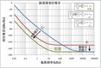
Figure 4: Schematic diagram of phase noise possessed by the wave source
(Schematic diagram of phase noise characteristics enclosed by green, red, and blue circles in the oscillator program block in the upper right corner)
Above, we have explained the phase noise characteristics of the wave source. As for the silicon resonator, the temperature characteristics of the silicon crystal itself vary greatly, and when constructing an oscillator, its temperature dependence must be compensated to ensure stability. For this reason, phase-locked loop circuits are often used as compensation circuits. Here, Figure 5 is used to illustrate the phase noise characteristics of a phase-locked loop circuit using a silicon resonator as the wave source.

Figure 5: Schematic diagram of phase noise characteristics of phase-locked loop circuit (left) and the tendency of phase noise characteristics caused by oscillator structure (right)
As shown on the left in Figure 5, a portion of the phase noise curve of the oscillator using a phase-locked loop circuit will increase. The principle of phase-locked loop circuit is to lock the wave source emitted by the voltage controlled oscillator (hereinafter referred to as "VCO") and output frequency doubling. Therefore, the phase noise characteristics of using phase-locked loop circuit are affected by two factors: VCO and phase-locked loop circuit. Usually, the phase noise characteristics of VCO as the wave source are worse than those of quartz wave sources, and will be displayed in the high-frequency field of phase-locked loop circuits, resulting in the above characteristics. Moreover, the frequency multiplication factor will also change the phase noise level of low frequencies, so the larger the multiplication factor, the worse the phase noise characteristics. The distortion caused by the phase-locked loop circuit and multiplication will also lead to the deterioration of the phase noise characteristics. Meanwhile, the characteristics of the high-frequency side depend on the output amplitude of the circuit and will remain constant regardless of the wave source.
Finally, summarize the phase noise characteristics of the fundamental oscillator with quartz crystal unit as the wave source, Si MEMS oscillator with phase-locked loop circuit using silicon resonator as the wave source, and medium voltage controlled oscillator with LC resonant unit as the wave source in Figure 5.
[The oscillator structure required for high-speed communication systems derived from phase noise characteristics]
The above section explains that the phase noise characteristics vary with different oscillator structures. When designing a system, designers should first decide whether to focus on the noise characteristics on the low-frequency side around the carrier wave (left in Figure 6) or on the phase jitter of 12k-20MHz in the communication loop bandwidth shown in SONET/SDH (right in Figure 6) when deciding on the electronic components, substrate layout, and design of dedicated integrated circuits to be used. Due to the phase-locked loop circuit of Si MEMS oscillators, a portion of the phase noise curve becomes larger and distortion occurs, while medium voltage controlled oscillators have frequency instability issues. Therefore, we believe that these high-risk products should not be used in the design of high-speed communication systems. The fundamental oscillator using quartz crystal units as the wave source has low phase jitter characteristics and stable frequency, making it more suitable for use in communication systems.
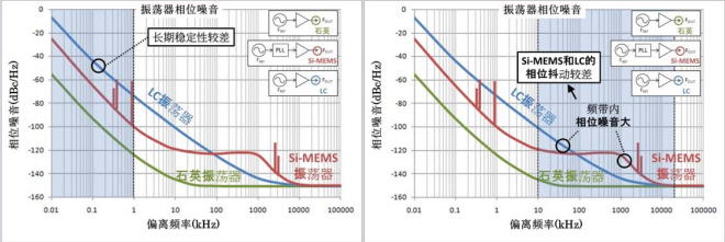
Figure 6: Comparison of low-frequency side characteristics (left) and high-frequency side (right) background noise characteristics around the carrier wave
Epson's oscillator products use quartz crystal units as the wave source, maintaining stable phase noise characteristics in the range of low-frequency to high-frequency background noise around the carrier wave. The circuit composition that starts with the fundamental wave is relatively simple, which can control the power consumption to a small extent. In communication systems with continuously improving communication speeds, we believe that fundamental oscillators using quartz crystal units as wave sources will become indispensable key components in communication systems. Epson will continue to develop products with the performance that customers pursue in the future, to meet their needs.