POP_UP_MESSAGE_CONTENT


Signal quality required for communication systems and reference signal sources (1)
【Composition of High Speed Communication System】
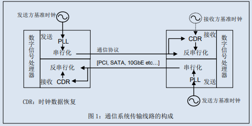
Firstly, Figure 1 illustrates the commonly used communication system transmission lines for transmitting data between two transceiver modules via various communication protocols such as PCI, SATA, or 10GbE. In such a system, an oscillator is used to generate a reference signal. Usually, the reference signal oscillates at a frequency lower than the data transmission rate. So, in order to generate serial data from the reference signal, the sender uses the Phase Locked Loop (PLL) circuit in the transceiver module to double the frequency of the reference signal to the desired frequency before sending. On the other hand, the receiver uses Clock Data Recovery, which contains a phase-locked loop circuit in the received data stream, to recover the reference signal, and uses the recovered reference signal to recover the data. In some high-end systems, the method of recovering data based on the reference signal held by the receiver is also adopted. As shown above, signal conversion and restoration are constantly carried out during the transmission and reception process. In increasingly high-speed communication, the receiver must correctly determine whether the received data is 0 or 1. Therefore, how to suppress the jitter and noise of the signal itself and improve the signal quality, and how to design the best transmission line specific integrated circuit are very important issues.

【Signal Quality Assessment Techniques】
When evaluating the quality of signals in communication systems, eye diagrams are often used. Eye diagram is a graphic formed by collecting a large number of high-speed digital signal waveforms using testing instruments such as oscilloscopes and superimposing them. It is named after the "eye" shape formed by the overlapping waveforms.
Assuming the communication protocol of the transmission line is 10GbE, the time (length) required to transmit 10Gbps signals in this system is 100 picoseconds per byte. When evaluating signal quality, overlap the signals that repeat every 100 microseconds to create an eye diagram. Assuming that the reference signal is pure and the dedicated integrated circuit design of the transmission line is good, an almost completely overlapping waveform as shown on the left in Figure 2 can be obtained. On the contrary, if there is a lot of noise and jitter in the reference signal, or if there is a loss such as insufficient bandwidth of the transmission line due to the design of the dedicated integrated circuit, the signal waveform will become unstable, and the overlapped waveform will show a situation where the eyes gradually close as shown on the right in Figure 2.
When determining whether the signal data is 0 or 1, it is important that the length and width of the eye opening are sufficiently large.
The reduction of the open eye due to noise and jitter will result in the receiver being unable to accurately determine the signal data, leading to an increase in BER. Almost all communication systems now require a BER of at least 1 × 10-12. This means that 1 byte of error is allowed for every 1012 bytes of data transmitted.
In summary, various information about signal quality such as noise, jitter, or insufficient frequency band can be obtained from the eye diagram.

[Elements that make up jitter]
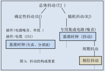
Figure 3 illustrates the constituent elements of jitter in a communication system. The total jitter TJ is represented by the sum of deterministic jitter DJ and random jitter RJ. Deterministic jitter refers to jitter caused by circuit design, electromagnetic induction, or external factors. The characteristic of deterministic jitter is that the frequency spread remains constant and is independent of time variation. The performance of the oscillator as a reference signal source is affected by distortion and subharmonics that affect deterministic jitter.
Random jitter truly represents unpredictable jitter components. It is naturally generated due to the characteristics of the components themselves, thermal noise, and other factors. The characteristic of random jitter is that it spreads over time. The jitter of the reference signal source affects the random jitter in the oscillator performance as a reference signal source.
Factors in other systems are also classified as causes of jitter, such as power supply noise and crosstalk of plugins, insufficient frequency band caused by cable design, etc., which are the causes of deterministic jitter, while noise from dedicated integrated circuits is the cause of random jitter. Therefore, system designers need to reduce overall jitter by improving the design of application specific integrated circuits, changing substrate layouts, and modifying components.

【Structure and characteristics of oscillators (reference signal sources) sold in the market】
Firstly, readers should have understood that in order to maintain signal quality, it is necessary to choose a reference signal source with less noise and jitter impact. Here, we will explain the structure (type) and characteristics of oscillators currently sold in the market.

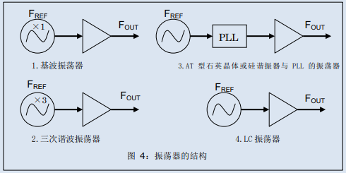
The oscillators currently sold in the market can be roughly divided into four types, with their structures shown in Figure 4.
The first type is the most common fundamental oscillator. The noise, jitter, and distortion characteristics of this oscillator are extremely superior, providing all the features of high precision and high performance. Its circuit composition is relatively simple, so it can control the power consumption to a small extent.
The second method is to use oscillators with third harmonic. The method used in the circuit design of harmonic oscillation is to use a filtering circuit to reduce the negative resistance of the fundamental wave, and generate negative resistance at a frequency that is a required multiple (here three times). This method can obtain high-frequency output that is difficult to obtain in the case of fundamental oscillation, and can maintain a high Q value, thereby achieving good low carrier phase noise. However, due to the complexity of circuit design (adjustment), this method also has the disadvantages of increased power consumption and decreased frequency variability caused by an increase in capacitance ratio.
The third method is to use an oscillator with a phase-locked loop circuit. This oscillator uses a quartz or silicon resonator as a reference signal source to emit an input signal, generates a synchronization signal of the input signal using a phase-locked loop circuit, and outputs the necessary frequency. Therefore, the advantage of this method lies in the convenience of using phase-locked loop circuit technology to obtain any frequency and the ability to provide high frequencies. However, its complex circuit structure leads to an increase in power consumption, which also has a negative impact on noise and jitter performance. We have previously introduced that in the case of using silicon resonators, due to the poor temperature characteristics of the silicon resonant unit, the temperature range that needs to be compensated is too large to perform analog temperature compensation. Therefore, phase-locked loop circuit technology must be used for temperature compensation. So, it is very disadvantageous in controlling the quality indicators of signal noise and jitter.
Finally, there is the LC oscillator. This oscillator, like a phase-locked loop circuit, is extremely convenient. After applying power, it outputs a larger amplitude and has a lower background noise. On the contrary, due to the low Q value of the material itself, the frequency stability and aging characteristics are poor, and there are also problems with low carrier phase noise.
As shown above, oscillators sold in the market have different structures, and suitable products should be selected according to their intended use. In response to these demands, Epson provides customers with oscillator products that already possess the phase noise characteristics, phase jitter, and distortion characteristics required as a reference signal source, in order to maintain the signal quality of customer communication systems.
【Introduction to Epson oscillators with low phase jitter suitable for communication systems】
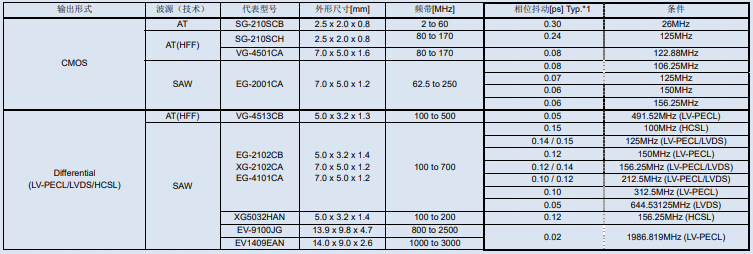
Epson has designated the fundamental oscillator (Type 1) as its main product and has formed a different product lineup with the required jitter performance for high-speed communication systems. Table 1 shows representative products among them.
We use quartz crystal units as the wave source in principle. Oscillators with frequencies below 80MHz use AT type quartz crystals, while those above 80MHz use High Frequency Fundamental (HFF) technology using inverted truncated AT type quartz crystals. We offer SG series oscillators and VG series voltage controlled crystal oscillators. We also offer EG and XG series SAW oscillators that use surface acoustic wave (SAW) technology and have the best jitter performance, as well as EV series voltage controlled SAW oscillators (VCSO). Moreover, we have prepared various outputs such as CMOS, LV-PECL, LVDS, HCSL, etc., all of which maintain the excellent advantages of quartz itself and have the ability to charge
Product specifications that meet the signal quality requirements of customers for various purposes.
Table 1: Epson oscillator product lineup and phase jitter strength data

*1: The phase jitter represents the deviation of the number (Typ.) from the frequency shown in the condition column by 12kHz to 20MHz, which was tested and calculated by our company.
In the future, Epson will expand the SG series with differential output and add new lineups such as SAW oscillators that can handle multiple outputs, continuously providing products with excellent performance in terms of jitter and noise to meet the necessary conditions as a reference signal source.


