POP_UP_MESSAGE_CONTENT


The characteristics of the real-time clock module with built-in digital TCXO in crystal RTC
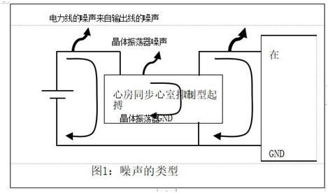
1. Noise generated by power lines
2. Noise generated by output lines
3. Noise generated by crystal oscillators
What is commonly referred to as "noise" is the cumulative result of these three factors.
Below we will explain each type of noise.
1. Noise, voltage ripple, and switch noise from power lines are typically emitted by power line trajectories.
This type of noise will affect the output of the crystal oscillator. In addition, it is necessary to ensure that the ripple noise generated by the crystal oscillator does not
Inflow into power lines. The implementation of these measures also improves isolation and prevents external noise generated by other devices from flowing into the crystal oscillator, thereby ensuring the stability of the crystal oscillator.
2. Output line noise
Output line noise refers to the signal output by a crystal oscillator, where the output line serves as an antenna. The output signal and
Physical tracking.
3. Crystal oscillator IC noise
Crystal oscillator integrated circuit noise refers to the noise emitted by the integrated circuits and wiring inside the crystal
Resolving this noise in an oscillator requires ensuring a stable power supply for the crystal oscillator and ensuring the formation of the required waveform to achieve stable operation of the crystal oscillator. These noise sources depend on the above reasons and can be indirectly mitigated through the power line and output line technologies mentioned later in this article.
The noise level emitted from the above sources is proportional to the current and current loop path. Therefore, a decrease in current or current loop path impedance will lead to a decrease in the level of emitted noise.
Generally speaking, there is a correlation between current and the length of the current loop path, as it is related to the crystal oscillator and its peripheral circuits.
Current volume: power line=crystal oscillator>output line
Current circuit size: output line>power line>>crystal oscillator
The output line noise has the greatest impact on crystal oscillator circuits, followed by noise
The contribution of power lines. Compared to the noise from the other two sources, the noise level emitted by the actual crystal oscillator IC is usually much lower.
Noise countermeasures
So far, in these technical notes, we have checked the crystal oscillator and
Their peripheral circuits. Here, we explain the measures to reduce this type of noise. There are three main types of noise reduction measures:
1. Establish stable power and ground connections.
2. Install a filter to prevent noise from the power cord.
3. Configure a stable output line on the circuit board.
1. Stable power and ground connections
Stable power and ground connection refer to an extremely low level of impedance spanning a wide range
Frequency bands (especially high frequencies) and conductors that achieve uniform potential at all points of the bandwidth. Specifically, the ground wire represents a
The circuit must therefore reach the maximum level of stability. This requires designing a ground plane with a wide surface area that does not shrink. On multi-layer boards, an additional ground plane is used to configure the power lines and ground wires on independent layers. When the design involves
The wider contact area of the weld ensures lower impedance, resulting in less noise. Do not place any signal lines, power voltage lines, or GND lines below the area where the oscillator is installed, including any internal layers and the other side of the circuit board.
2. Power line filtering
The usual practice is to place a filter between the power line and the ground line to prevent noise from spreading out
The crystal oscillator does not leak into the power supply or ground wire, otherwise it is to prevent the generation of noise
The power cord enters the crystal oscillator. Usually, a bypass capacitor is used as a filter for power lines and grounding wires. The detailed explanation is as follows.
a. Bypass capacitor
A bypass capacitor can reduce the impedance of interactions and help stabilize the circuit
Operate while absorbing the noise present on the power line. This is a well-known type of noise
The elimination method of installing a capacitor with an appropriate capacitance value will solve most noise related problems.
i. Capacity value of bypass capacitor
The standard bypass capacitance value is 0.01 μ F and 1 μ Between F. The value should be set as low as possible, but within the range of the VCC at the power terminal and the impedance of the power line
The relationship with the ground is a frequency, which is three times the frequency of a crystal oscillator.
Here, you must confirm the frequency characteristics at this capacity to ensure that the impedance level on the high-frequency side or low-frequency band side will not be affected
Ii. Install bypass capacitors
To reduce noise, bypass capacitors should be installed as close as possible to the crystal oscillator. As the trajectory length increases, parasitic inductance will increase and cause an increase
Impedance at higher frequencies. The trajectory length of the bypass capacitor should be configured to allow the signal to pass through the connection with the power line. This will force noise to pass through the bypass capacitor, improving the noise cancellation effect.
Avoid using the stratigraphic type shown in Figure 2a. When installing bypass capacitors. High frequency noise usually propagates in a straight line, so the noise does not pass through a bypass
3. Configure a stable output line
A stable output line refers to the trajectory that can effectively transfer the output waveform of a crystal oscillator to the desired input with minimal distortion and electromagnetic emission.
The key to configuring a stable output line is to ensure waveform characteristics, such as TR, TF
VOH, VOL, etc. need to be inputted. In addition, a stable output line needs to be eliminated
Unneeded signals, such as overshoot, undershoot, ringing, and echo, are shown in Figure 3b. Equally important is to understand the efficiency of the tracking antenna to reduce unnecessary radiation.

Measures to prevent output waveform distortion include:
a. Configure serial resistance
b. Configure terminal resistance
c. Configure filters
d. Matched output line impedance
a. Configure series resistance
Connecting a crystal oscillator to an input device typically results in waveform distortion, including overshoot, undershoot, and ringing. These distortions contain high-frequency components that are 3-7 times higher than the oscillation frequency and cause emission
The noise that should be eliminated. To eliminate this distortion, we connected a serial resistor
Between the output terminal of the crystal oscillator and the output line, as shown in Figure 4. The resistance value is configured so that the sum of the output impedance (Ro) and serial resistance (Rs) of the crystal oscillator is equivalent to the output line impedance (Z0).
Testing can be conducted to determine the optimal value of series resistance. test
This method involves measuring the output waveform with an oscilloscope and converting the serial resistance from low to high values. The optimal resistance value is at
The overshoot, overshoot, and ringtone have all been eliminated.

b. Configure terminal resistance
The configuration of terminal resistors largely depends on the type of interface and the type of clock wire used. The configuration will vary based on these factors.
In general, when there is a mismatch between the two, the output waveform will be distorted
The impedance of the output line and the impedance of the device input. When the impedance is not
When matching, the traveling wave cannot be fully received, and some signals are reflected back to the oscillator, resulting in distortion of the output waveform. This can lead to high-frequency noise.
When the branch crystal oscillator outputs to multiple devices, this waveform distortion can lead to triggering errors. Therefore, appropriate termination and impedance matching are crucial.
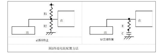
To prevent echoes from the receiving device, the input should terminate at the same impedance value as the output line. Figure 5 shows two common termination methods: split termination and communication termination.
c. Filter configuration
Usually, output waveform distortion can be solved using serial resistors or terminals
Resistance filtering is used in situations where these methods cannot solve the problem. The use of filters is an effective method to eliminate high-frequency noise, but this method increases TR and TF (waveform dissipation). Therefore, you must choose a filter that is suitable for the tr and tf attributes. In addition, using a larger capacitor as a filter can lead to an increase in
The flow of current, conversely, can also lead to an increase in noise.
d. Output line impedance matching
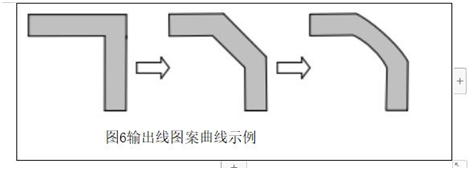
Reducing the waveform echo on the output line requires the impedance of the output line to be as consistent as possible. As shown in Figure 6, consistent output line impedance has been achieved
It involves configuring output line pattern curves to convert right angles to 45 º angles, and if possible, to circular curves. Additionally, please avoid using through holes or T-branches.
Finally, we will introduce the two most important methods for reducing noise emissions.
a. Use shorter output lines
Among all circuits, the output line is the most prone to generating noise. Therefore, in the design and
When laying out, high priority should be placed on allowing the shortest output line to have no impedance
Fluctuate by using shorter circuits to adjust the resonant frequency of the output line to a higher level
In terms of frequency. The higher the frequency, the greater the damping of the output frequency component, resulting in a smaller noise emission.
b. Using a shorter current cycling path
As mentioned above, the noise level emitted from the output line is proportional to the current
Loop path length. Therefore, the output of the crystal and the ground trajectory are important
The oscillator and input device should be as short as possible. A simple way to achieve this is to install the ground plane on the other side of the output trajectory.
As mentioned above, careful circuit design of crystal oscillators and their peripheral circuits is crucial for noise reduction. Optimized circuit design allows for the avoidance of noise related issues and enables them to
Equipment to achieve its full performance potential.
[3] Peripheral circuit of crystal unit
1) Crystal unit and peripheral circuit mounting surface
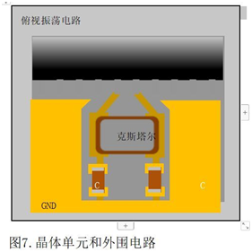
Please arrange crystal units, capacitors, and resistors near the IC as much as possible. Try to keep the line as short as possible and avoid crossing with other signal lines.
As shown in Figure 7, it is recommended to provide a wide GND area on the same surface of the board where the crystal unit is installed.
Resistors Rd and Rf are omitted in Figure 7.
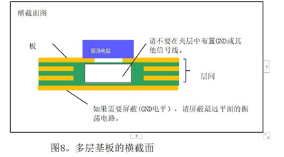
2) Cross section of multi-layer substrate
As shown in Figure 8, for multi-layer PCB boards, do not place other signal lines under the crystal unit.
If GND shielding is required, shield the surface farthest from the oscillation circuit.
[4] At the end
Please note that the content described here is a reference example for the peripheral circuit design of crystal oscillators and crystal units, and cannot be guaranteed.
For crystal units, we suggest that you also refer to the design guidelines of oscillation circuit manufacturers.


