POP_UP_MESSAGE_CONTENT


Explanation of Low Jitter Technology for Programmable Oscillators
[Development goal for low jitter]
Generally speaking, low jitter characteristics can be achieved through designs with high SPXO current consumption. This is because the circuit design that increases the signal level of the oscillator circuit increases current consumption, improves signal-to-noise ratio (SNR), and ultimately improves jitter caused by noise. as long as
The design is based on this trade-off, where current consumption must be high to achieve low jitter characteristics.
To offset the above trade-offs, we used the FoM (performance chart) as an indicator as shown in the following formula. This equation uses "phase jitter" instead of balancing jitter characteristics and current consumption
"Electricity consumption" and normalize it.
FoM [dB]=20 log (1 (Ji) t [(t) s (e)] (r))+10 log (1P [(o) mW (wer)])
The P-SPXO SG-8101 series has FoM=-200 dB, and our SPXO has better jitter
Performance vs. foam=-240 dB. By setting development goals to reduce the FoM of P-SPXO, it will lead to a
Basic performance improvements. We have set a new P-SPXO development goal, which is FoM=-225 dB. this
Correspondingly, our low jitter PLL oscillator uses an integer type PLL. However, integer PLL is limited to integer multiples of built-in crystal units. Therefore, we set the goal for FoM, which is equivalent to an integer type PLL, by using a fractional number type PLL that can be freely set at any frequency. In addition, our goal is to
Miniaturization and high precision to meet market trends and achieve high efficiency
Compact and precise. Specifically, our initial development goal is to reduce the area ratio by 64% and expand the upper limit of the operating temperature range from+105 ° C to+125 ° C
The current SG-8101 series. As a result, the goal of FoM=-225 dB was achieved. We have successfully broken it
Balancing and commercializing small P-SPXO, SG-8201 series, with low current consumption and low jitter
characteristic

PLL circuit as reference clock
Target frequency and output
The current generated by the crystal oscillator is input into the PLL circuit, which can be adjusted according to the division ratio of the PLL circuit's divider
Identify which part of the PLL circuit is involved
The deterioration of jitter characteristics caused by PLL circuits, and its improvement will lead to the implementation of jitter characteristics
The goal of development is to break the balance between jitter characteristics and current consumption.
Sand scab low shake technology
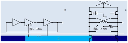
VCO is an oscillator whose frequency can be controlled by the control voltage. There are two types of VCO circuits,
One is ring VCO, and the other is LC VCO. The respective circuit configurations are shown in the figure. 3 and 4

The ring VCO has a circuit configuration where an odd number of inverters are connected to apply positive feedback,
And control the frequency by changing the current provided to the inverter based on the control voltage.
The circuit size is small, the current consumption is low, but the impact on jitter characteristics is relatively small. Our P-SPXO SG
The 8101 series adopts ring VCO, and the development goal is to prioritize the characteristics of small size and low current consumption. On the other hand, LC VCO has a circuit configuration that oscillates through LC resonance, and controls frequency by applying control voltage to the variable capacitor and changing the capacitor. Due to the excellent jitter characteristics of LC VCO, we are attempting to achieve our development goals through LC VCO. However, the integrated coil has a problem as it occupies a larger area of the integrated circuit compared to a ring VCO. If the coil is designed smaller, the inductance value will also be smaller, thereby increasing the current consumption of VCO To address this issue, we focus on reducing the Q and inductance values of the coil due to eddy currents generated by surrounding conductors. We have studied a method to suppress eddy currents. By using an electromagnetic field simulator to inspect various wiring shapes and finding a design that minimizes the Q value, the coil footprint is minimized as much as possible. After making a prototype in our FAB to confirm the actual effect of the IC, we found that it can be used
LC VCO achieves reduced jitter.
Realize small precision, high precision, and low jitter
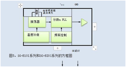
Our development goals include "small" and "high precision", as well as low jitter. Therefore, it is necessary to make it smaller than the IC size of the SG-8101 series to adapt to the target size of SG development
8201 series. Figure 5 shows the block diagrams of the SG-8101 series and SG-8201 series.

Although LC VCO has been successfully miniaturized, it is still larger in area than the ring VCO used in SG -
8101 series, so it is necessary to miniaturize other circuits besides PLL. Temperature compensation circuit
Occupying the second largest area after PLL. The temperature compensation circuit is an important factor in achieving this goal
High precision, especially to adapt to higher operating temperatures of+125 ° C. Miniaturization is
We need it here, so we have decided to completely change the traditional
The frequency temperature characteristics of AT cutting crystal units follow the characteristics of a cubic curve.
The temperature compensation circuit generates a voltage, reproduces the cubic curve, and changes it
The frequency of the oscillator cancels out the frequency temperature characteristics of the crystal based on the voltage
The processing flow of generating cubic curve voltage by significantly reconsidering the unit
Temperature compensation circuit, we have achieved a reduction of approximately 20% in circuit area
Ensure a solution to the compensation plan.
In addition to the development of the aforementioned technologies, we also reviewed the design of frequency control
The circuit layout can be further optimized to reduce the size of integrated circuits and improve jitter. Therefore,
We achieved the development goal of FoM=-225 dB, overcame trade-offs, and achieved significant results
Between jitter characteristics and current consumption, achieving small and high accuracy.
[Compared to traditional products]
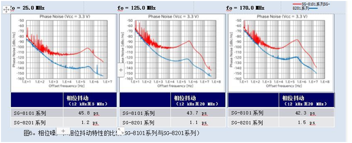
Figure 6 shows the phase noise and phase jitter characteristics of the SG-8201 series. Compared to SG-8101
In the series, it achieved a significant reduction in jitter.

all in all
The P-SPXO SG-8201 series has the characteristics of low jitter, small size, and high accuracy
For various applications and to help maximize the product value of customer products. Seiko Epson will continue to operate
Develop crystal devices that can enrich society.


