POP_UP_MESSAGE_CONTENT


Reference plane analysis of high-speed and RF RF signals
For an electronics enthusiast, the issue of reference planes in PCB design often confuses many people. As is well known, the power plane can be used as a reference plane, and common 6-layer boards generally use the power layer as the reference plane for DDR signals. However, can high-speed and RF signals also use the power layer as a reference plane? Today we will discuss it together.

Regarding the reference plane
What is a reference plane? As the name suggests, it is a plane. To understand this plane, one must first understand the concept of transmission lines. We all know that transmission lines must be used to analyze signal transmission on PCBs to explain various phenomena in high-speed circuits. The simplest transmission line includes: signal path and reference path (also known as return path). Signals are transmitted in the form of electromagnetic waves on transmission lines, and the signal path and reference path constitute the transmission environment of electromagnetic waves; From the perspective of the current circuit, the signal path carries the signal current, while the reference path carries the return current. Therefore, the reference path is also known as the return path.
As for the wiring on the upper layer of the PCB, the wiring and the planar layer below constitute the physical environment for electromagnetic wave transmission. The signal path is the surface wiring, so the planar layer below is the reference path. For this special structure on the PCB, the reference path appears in the form of a plane, so it is also called a reference plane. It doesn't matter what network properties the plane below the wiring has here, VCC、GND、 Setting up an isolated copper sheet without a network is also possible, the key is that the underlying plane is a conductor. The following figure shows the field distribution and current distribution of surface wiring:
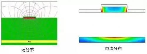
In terms of inner layer routing, the routing, upper plane, and lower plane constitute the physical environment for electromagnetic wave transmission, so both the upper and lower planes are reference paths for signals, that is, reference planes. The following figure shows the field distribution and current distribution of the inner layer wiring:
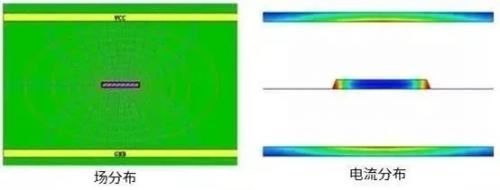
From the figure, it can be clearly seen that if the distances between two planes and the wiring are approximately equal, then the two return circuits are also approximately equal. At this point, both planes are equally important, so it is not difficult to understand that the upper and lower planes of the inner wiring are both reference planes.

There are two points in the reference plane: calculating impedance and providing a return path. Therefore, if only the requirement of consistent impedance is met, both the GND plane and the power plane can be used. However, in general, the reference plane is mainly used as a path for current return, so there are the following issues.
1. How is the signal referenced to the power plane?
As analyzed earlier, the power layer can also be used as a reference plane to calculate impedance. Now, we will analyze it from the current return path. Taking a simple 4-layer PCB as an example, the signal passes through the through-hole replacement layer reference power supply, and its signal return path is as follows:
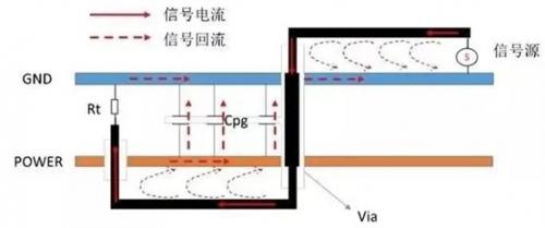
When a high-speed signal propagates on a signal line, due to capacitive coupling between reference planes during the forward propagation of the signal, when dV/dt occurs, there will be a phenomenon of current flowing through the coupling capacitor to the reference plane, and transient current will flow back to the source circuit below the transmission line. When the power layer is used as a reference plane, the signal return will first flow to the power layer, then flow to the ground network through the Cpg between the power and ground networks, and finally flow to the source circuit through the ground layer, forming a complete power circuit. Controlling the impedance of the high-speed signal loop is crucial as it directly affects the signal transmission characteristics.
2. Can high-speed signals refer to the power layer?
In theory, just like the ground plane, the power signal layer can also be applied to low impedance signal return paths. Assuming there are enough bypass capacitors, the power plane transmission will be as good as the ground, and a strip transmission line can also work on one power plane and ground plane or two power planes.
However, when the signal references the power layer, the capacitive channel between the Cpg power supply and the ground network has the greatest impact on the signal in the return path. It may be a complex decoupling capacitor distributed on the power supply ground network, or it may include flat capacitors between the power supply ground planes. Due to its complex composition, the impedance characteristics exhibited at each frequency point are different, making it difficult to quantify and control. Therefore, this assumption is difficult to hold. Even if the power layer is closer to the signal layer, the return signal will still pass through the power layer and return to the formation, because the signal input is based on the formation as the reference layer.
But if decoupling is not done well, the impedance between the power layer and the formation will be very high, and the return signal will be subjected to a large impedance. The signal reference power layer will have an impact on signal quality, and the impedance between power layers is the main factor affecting it. The higher the signal frequency, the more obvious the impact will be. Of course, not all signals cannot be referenced to the power supply. The specific frequency and signal that can be referenced to the power supply depend on the actual PCB design and the actual situation of the PDN network. It is best to use simulation software for analysis and verification.
Why do some signal designs require reference to their own power layer? This is because the internal signal of the chip is referenced to the power supply, so it is better to reference the power supply on the PCB. However, most chips are designed with reference ground for high-speed signals, so reference ground is recommended in most high-speed signal design guidelines. Although the decoupling capacitor of the high-frequency power supply shows low impedance characteristics and the power supply and ground exhibit equipotential, the placement of the decoupling capacitor may increase the signal return area, thereby affecting signal quality. Therefore, for most high-speed signals, reference ground is recommended. Here is a suggestion: For high-speed signals, it is recommended to refer to the ground plane, which should have at least one complete ground plane; In addition, the power plane needs to be tightly coupled with the ground plane, that is, closely together.
3. Can RF signals refer to the power layer?
The theory of whether high-speed signals can refer to power signals can also explain the question of whether RF RF signals can refer to the power layer. From the perspective of the return path, RF RF signals are even less suitable for referring to the power layer. The reason is that poor impedance and coupling between the power layer and the geological layer can have a significant impact on RF signals. It should be noted that the power layer is not the true ground, and from an EMI perspective, it is not recommended to use the power layer as the ground for microstrip lines, as the signal return path may become very long and be interfered with. Secondly, both the power supply and the ground plane can serve as reference planes and have a certain shielding effect, but relatively speaking, the power supply plane has a high characteristic impedance and a large potential difference from the reference level. From the perspective of shielding, the ground plane is generally grounded and used as a basic level reference point, and its shielding effect is much better than that of the power plane.


