POP_UP_MESSAGE_CONTENT


The key "hand" in semiconductor wafer testing, where does the ceramic substrate play a role?
In recent years, with the continuous improvement of semiconductor process technology and the shrinking of process nodes, there are over one billion transistors on a single chip. The development of advanced processes is accompanied by the semiconductor industry's pursuit of yield and cost.

Wafer sorting process
In the semiconductor manufacturing industry, the integrated circuit (IC) production process can be divided into four stages: Product Design, Front End Manufacturing, Back End Packaging and Testing, and subsequent Board Assembly. The circuits validated through design are mass-produced on wafers in a wafer fab. It is necessary for wafer fabs responsible for front-end manufacturing to ensure the quality of chips with such a large number of transistors through testing and analysis.
The "Fingertip" of Wafer Inspection Equipment - Probe Card
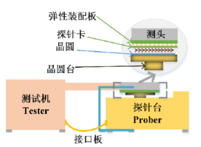
The main method of wafer testing is through the linkage between the testing machine and the probe station. During wafer testing, the tested object is placed on the probe station, and then the probe on the probe card is directly in contact with the pad or bump on the chip, allowing the testing machine and chip to communicate directly. The test signal measured by the probe is then sent to the automatic testing equipment (ATE) for analysis and judgment, thus obtaining the electrical characteristic test results of each grain on the wafer.

Schematic diagram of wafer testing equipment
Probe cards are key tools for wafer functional verification testing and industrial testing, which can help engineers better understand the performance and working principles of chips, thus enabling better design and improvement. At the same time, the probe card can also help engineers quickly confirm whether the chip meets the specification requirements, so as to adjust it in a timely manner during the research and development process. In addition, its application in chip testing can reduce the cost of chip packaging and is also considered the "fingertip" of wafer testing equipment.
Potential ceramic material application market in probe cards
In the entire probe card, STF substrates are the core components. The spatial conversion substrate plays a role in the electronic connection spacing conversion and electrical signal transmission throughout the probe card, while providing sufficient mechanical/mechanical strength to support the forces of hundreds to thousands of newtons applied during the testing process.
With the continuous development of China's integrated circuit manufacturing industry, considering process optimization, quality control, and cost, more and more wafer testing has introduced temperature rise and high temperature testing. Compared to room temperature testing, this type of probe card is affected by the substrate material, especially in multi temperature zones where deformation occurs at high and low temperatures. The deformation of the probe card can cause the displacement of the probe trace. The offset of the needle marks usually leads to poor contact between the probes on the probe card and the pads (pads) on the wafer, resulting in unstable testing and affecting testing time and quality. Excessive needle offset can damage the internal circuit of the wafer when the probe comes into contact with the wafer PAD, resulting in scrap and economic losses. At the same time, the probe card will also be scrapped due to its inability to perform wafer testing.
The adapter board in high-end probe cards often uses ceramic substrates. Precision ceramic substrates have excellent electrical insulation, high thermal conductivity, high adhesion strength, and large current carrying capacity. And it has high strength, high hardness, a wide temperature range for use, and can reach -55 ℃ to 850 ℃. Its thermal expansion coefficient is close to that of silicon chips. In a multi temperature zone testing environment, it is one of the effective solutions to solve deformation.

Ceramic substrate for probe card
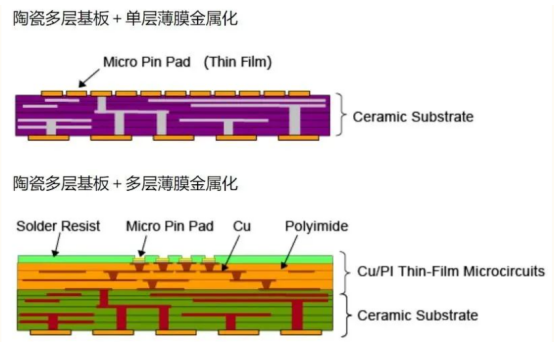
The ceramic substrate used for probe cards is generally a multi-layer ceramic substrate with metalized single-layer or multi-layer thin films. The multi-layer ceramic substrate is made by laminating high-temperature or low-temperature co fired ceramics through multiple layers and co firing, and is commonly referred to as a multi-layer ceramic space conversion substrate (MLC).
During the assembly process, there are measuring heads with tens of thousands of miniature contact pins that are guided through the silicon nitride plate. The needle contacts the surface of the chip and is used to exchange signals with the testing system, which then checks the functionality of the chip. The silicon nitride plate fixes the needle in the correct position to ensure error free measurement. At the same time, the contact pin must be able to bounce back along its longitudinal axis to ensure soft contact with the silicon surface. Silicon nitride must have excellent strength and high resistance to ensure panel stability and avoid interference with signal transmission. In addition, laser technology is required to create guide holes in the material, and the silicon nitride plate must be thin. The compact development of Starceram N3000 P high-performance ceramics combines necessary strength, low wear, and the ability to slide back and forth in guide holes; The measurement tolerance for material thickness is only ± 1 µ m, and the maximum size can reach 190 mm x 190 mm without damaging the edges.
In addition to silicon nitride, there are also high alumina ceramics. High alumina porcelain is a ceramic material mainly composed of alumina, which has excellent electrical properties and high temperature stability, and has been widely used in probe cards. Although high alumina ceramics have high hardness and strength, they are too brittle. In addition, ceramic materials such as boron nitride, silicon carbide, and magnesium oxide can be used for probe cards, and the application needs to be selected according to the specific performance requirements of the usage environment


