POP_UP_MESSAGE_CONTENT


Chip manufacturing process: crystal growth, forming
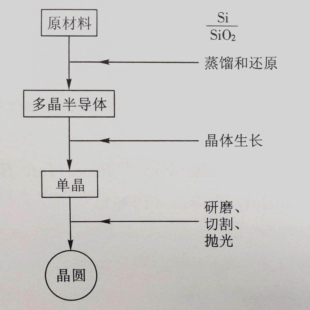
2. Growth of monocrystalline silicon
The basic technique for growing single crystal silicon from liquid molten silicon is called Czochralski method. More than 90% of monocrystalline silicon in the semiconductor industry is prepared using this method.
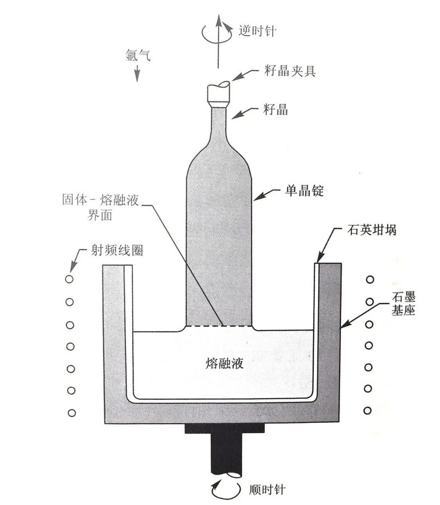
During the crystal growth process, polycrystalline silicon is placed in a crucible, which is heated above the melting point of silicon. A seed crystal with an appropriate crystal orientation is placed in a seed crystal fixture and suspended above the crucible. Insert the seed crystal into the molten liquid. Although the seed crystal will partially melt, the top of the unmelted seed crystal will come into contact with the surface of the molten liquid. Then slowly pull up the seed crystal, and the molten liquid gradually cools on the solid-liquid surface, producing a large single crystal ingot.
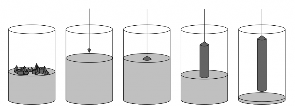
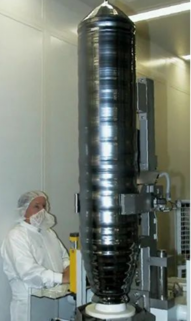
The standard crystal pulling rate is several millimeters per minute. If you want to draw a larger diameter monocrystalline silicon ingot, you can apply a magnetic field to a basic Czochralski machine. The purpose of applying an external magnetic field is to reduce defects, impurities, and oxygen content. The single crystal silicon ingot grown by Czochralski method is shown in the figure:
Doping:
During crystal growth, a certain amount of impurity atoms can be added to the melt to obtain the desired doping concentration. For silicon, boron and phosphorus are the most commonly used doping materials for forming P-type and N-type semiconductors, respectively.
To achieve a uniform doping distribution in the ingot, the pulling rate can be increased and the rotation rate can be reduced. Another method is to continuously add high-purity polycrystalline silicon to the melt during the single crystal growth process, so that the initial doping concentration of the melt remains unchanged.
3. Growth of higher purity monocrystalline silicon
The zone melting process can grow higher purity single crystal silicon. The device is as follows:

A high-purity polycrystalline silicon rod with seed crystals at the bottom is kept vertically and rotated. This polycrystalline silicon rod is sealed in a quartz tube filled with an inert gas (such as argon).
During the operation, a small area (approximately a few centimeters long) of the polycrystalline silicon rod is melted using an RF heater. The heater is moved upwards along the axial direction of the polycrystalline silicon rod, causing the float zone to move upwards and sweep across the entire polycrystalline silicon rod. The suspended zone melted silicon is supported by the surface tension between the melting silicon and the recrystallized solid silicon. When the floating melting zone moves upward, the retreating end recrystallizes and grows a single crystal with the same orientation as the seed crystal.
The use of zone melting method can grow single crystal materials with higher resistivity. Therefore, the single crystals produced by zone melting method are mainly used for manufacturing high-power, high-voltage devices, etc. This growth technique can also be used to remove impurities, known as zone melting purification technology, which can be used to provide extremely pure raw materials.
4. Wafer Forming: Cutting, Grinding, Polishing
After the crystal growth is completed, the first forming operation is to cut off the head of the ingot containing the seed crystal and the final solidified tail. Then polish the surface to determine the diameter of the wafer. Then grind one or several planes along the axis of the ingot. These planes are used to indicate crystal orientation and conductivity type. The largest plane is called the main grinding surface, which can be used to automatically fix the position of the wafer and determine the orientation of the device relative to the crystal by referring to the mechanical orienter in the automatic process equipment. Other smaller surfaces are called secondary grinding surfaces, which are used to indicate crystal orientation and conductivity type.
-Then the ingot is cut into wafers by diamond blades. Cutting determines four wafer parameters: ① crystal orientation of the crystal plane, such as<111>or<100>; ② The thickness of the wafer, such as 0.5~0.7 mm, is determined by the wafer diameter; ③ The tilt of the crystal plane refers to the difference in thickness from one end of the wafer to the other; ④ The curvature of a wafer refers to the degree of curvature from the center to the edge of the wafer.
After cutting, both sides of the wafer need to be ground with a mixture of alumina (Al2O3) and glycerol, which can generally be ground to a flatness of 2um. This grinding operation usually causes damage and contamination to the surface and edges of the wafer, and the damaged and contaminated areas can be eliminated by chemical etching.
The final process of wafer forming is polishing, which aims to provide wafers with highly flattened and clean surfaces for subsequent photolithography processes.
5. Crystal characteristics
Defects:
Actual crystals always have defects, which affect the electrical, optical, and mechanical properties of semiconductors.
Point defects are particularly important in the study of oxidation and impurity diffusion processes.

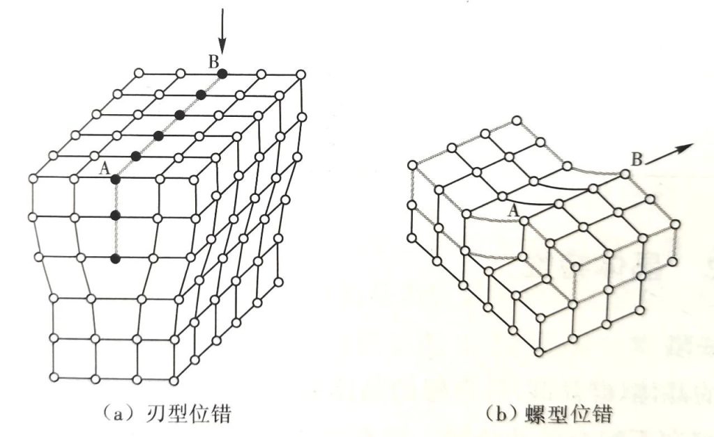
Line defects: Semiconductor devices should try to avoid line defects as much as possible, because metal impurities are prone to precipitate at the line defects, thereby reducing device performance.
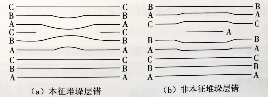
Surface defects: Crystals with surface defects cannot be used to manufacture integrated circuits and can only be discarded.
Comparison of Material Characteristics:
Comparison of the Characteristics of Silicon Materials and the Requirements for Wafer Manufacturing in ULSI (Ultra Large Scale Integrated Circuit):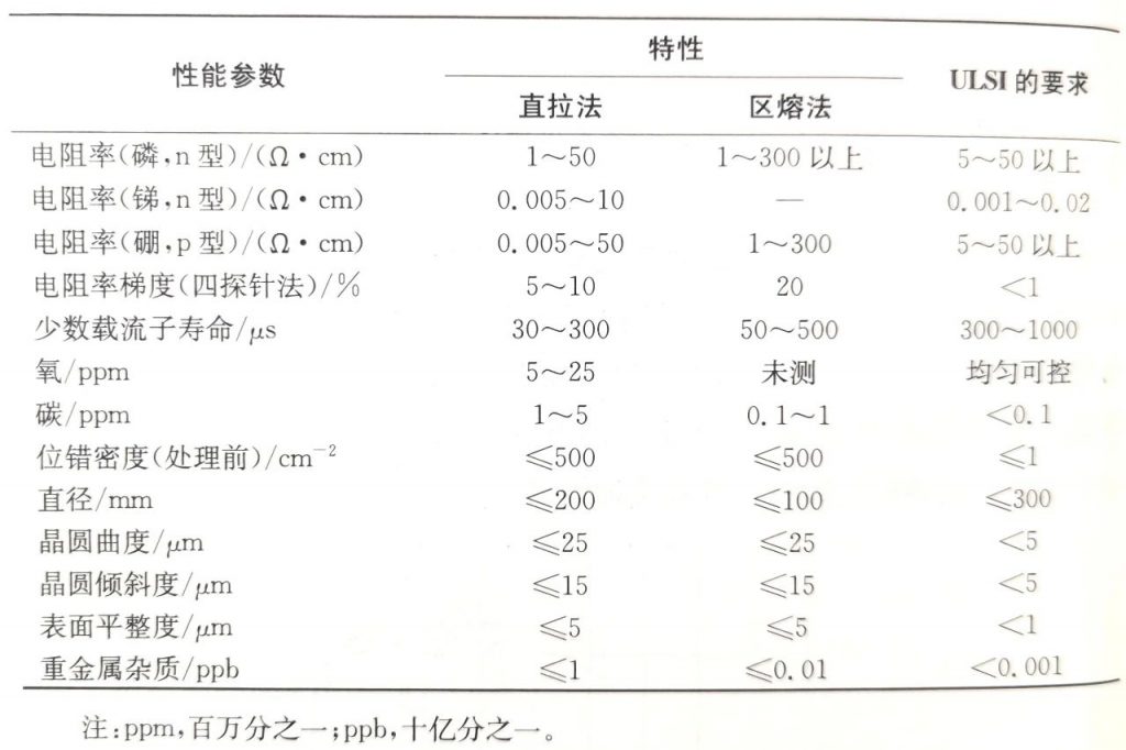
Characteristic measurement method:
The resistivity can be measured using the four probe method.
For small amounts of impurities, such as oxygen and carbon impurities in silicon, secondary ion mass spectrometry analysis can be used to determine them.


