POP_UP_MESSAGE_CONTENT


SD2058 FAQ
3. Q: Why can't I detect SD2058 and return an ACK when using the emulator for single step debugging?
A: Because the I2C bus of SD2058 has a 0.5s timeout automatic reset function.
4. Q: Why is there a jump in time when reading from RTC. If it jumps directly from 9 seconds to 16 seconds, and it will be greater than 60 seconds?
A: RTC uses BCD code for timing, where 0x10 represents 10 seconds in decimal. When viewed in decimal, it shows a jump from 9 to 16 (0x10=16).
5. Q: Why do I sometimes read the time in garbled characters?
A: 1.SD2058 has completely lost power, and the time it reads when powered on again is a random number (possibly garbled);
2. The VBAT foot of SD2058 may also read garbled characters when suspended;
3. The overall speed is too fast or there are non-standard aspects in the timing of the communication program (see appendix);
4. Control the multiplexing of the IO ports of SCL and SDA;
5. The SDA port of the chip is not equipped with a pull-up resistor.
6. Q: Why do hours run until 25 o'clock, 26 o'clock?
A: The 12/24-hour clock is not set correctly. Set the 12/24 hour clock at the highest bit of the hour register (02H).
7. Q: Why does the hour display 90 o'clock, 91 o'clock?
A: After reading the hourly data, the highest bit (12/24 hour control bit) was not masked.
8. Q: When SD2058 generates interrupt output, is the INT pin high or low?
A: The INT port is an N-channel open circuit output port, usually connected to a pull-up resistor during use. When there is no interrupt output, it is high level, and when an interrupt occurs, it becomes low level.
9.Q:Can the INT foot of SD2058 be suspended when not in use?
A: It's possible.
10. Q: What is the reason why SD2058 does not vibrate?
A: 1.There is leakage between the two legs of the crystal oscillator due to wiring, contamination, condensation, and other reasons. Please wash and dry before trying again;
2. The wiring of the crystal oscillator circuit is too long. When wiring on the PCB, the wiring of the crystal oscillator circuit should be as short as possible and as close to the IC as possible;
3. The load capacitor or matching capacitor does not match the crystal oscillator or there is a problem with the quality of the capacitor (please refer to 11. Q);
4. The PCB board is damp, resulting in impedance mismatch and inability to vibrate;
5. There is a problem with the quality of the crystal.
11. Q: What size matching capacitor should be used for SD2058?
A: Crystals with a load capacitance of 6pf typically use a matching capacitance of 7pf; A crystal with a load capacitance of 12.5pf typically uses a matching capacitor of 15pf.
12. Q: The power consumption of SD2058 is very high, and the backup battery runs out quickly?
A: Under normal circumstances, the power consumption of SD2058 is approximately 1uA.
1. The pull-up resistor is connected to the battery terminal. You can refer to the application reference circuit introduced in the SD2058 manual;
2. It is possible that the chip has been damaged. Please replace the chip and check if it is functioning properly.
13. Q: Why can it be set up on February 30th? Can't the chip be fault-tolerant?
A: SD2058 does not have fault tolerance function, please make sure to ensure the writing time. Setting non-existent time or date data will cause the counter to fail to count properly.
14. Q: Does the 32K pin of SD2058 have an output when powered on? How to control its output and disable it?
A: When SD2058 is powered on, a 32K frequency square wave will be output from pin 32K, which is enabled through an internal register.
15. Q: Why didn't I measure the output waveform of pin 32K when I powered on SD2058?
A: Need to connect a pull-up resistor.
16. Q: Why can't SD2058 read only 12 bytes from the user RAM register? Isn't it 44 bytes?
A: Accessing the registers of SD2058 from 20H onwards does not return an ACK. Please do not judge the ACK returned by SD2058 when reading or writing addresses after 20H.
17. Q: After setting the year, month, and day for SD2058, can it automatically adjust the week?
A: The week system corresponding to the calendar cannot be automatically adjusted, and can be achieved through certain algorithms. Below is a commonly used formula:
A: The most common formula:
W = [Y-1] + [(Y-1)/4] - [(Y-1)/100] + [(Y-1)/400] + D
Y is the number of years, and D is the cumulative number of days on this day in the year, which is the day on which this day is in the year.
B: The best formula to use is the Zeisler formula:
W = [C/4] - 2C + y + [y/4] + [13 * (M+1) / 5] + d - 1
C is the century minus one, y is the last two digits of the year, M is the month, and d is the day. January and February should be calculated based on the 13th and 14th months of the previous year, and both C and y should be calculated based on the previous year.
The [...] in both formulas refers to taking only the integer part of the calculated result. What is the remainder of W divided by 7, which is the day of the week. If the remainder is 0, then it is Sunday.
18. Q: How to determine from software that SD2058 has lost power?
A: Read the 0FH register and check if the lowest bit (RTCF) of the register is 1. If it is 1, it indicates that SD2058 has lost power.
19. Q: Why can I read the time of SD2058 but not write the time?
A: SD2058 has three built-in protection soft locks (WRTC1~WRTC3), which need to be set to position 1 before writing to the registers. The unlocking order for setting 1 is: WRTC1->WRTC2, WRTC3; After the write register operation is completed, protect the register data with these three lock positions 0. The order of locking with 0 is WRTC2, WRTC3->WRTC1. You can refer to the demo routine on the relevant official website for details.
Appendix: Examples of Program Issues
When switching port directions, a STOP signal was introduced.
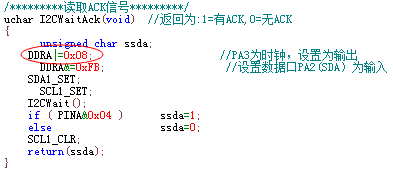
This function sets the input and output of the IO port from the beginning, and there was no error. SCL was low before this operation, but some microcontrollers set the SCL port to output, which causes SCL to become high. The problem is that when SDA is set as input, SDA will also change from low to high, forming a STOP signal. The bus is immediately released, and the previously sent data is cleared, so we cannot wait for an ACK response.
The SCL line has only one direction and is always the output. It only needs to be set once in the START function. The modification method is to mask the statement DDRA |=0x08.
2.Introducing START when sending the STOP signal may also cause the I2C slave device to malfunction.
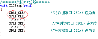
The function that sends the STOP signal above doesn't seem to have any errors, but if the SCL line is in a high state before calling this function, a START signal will be generated when the function starts calling. A safer approach is to first lower SCL, then lower SDA, and swap the positions of SDA1_CLR and SCL1_CLR.
3. Familiarity with the I2C protocol bus protocol resulted in a failure to read the specified address register.
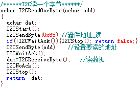
The above program seems to have no problem, but in fact, it does not understand the I2C transmission protocol. It assumes that after sending the read command, sending another address will read the data in the specified register. The correct timing diagram is as follows:

The address of the register is not sent out with a read command, but with a write command. The correct way to write it is as follows:
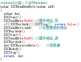
4. If the holding time of the start signal, data establishment, or data retention is too short, it may cause the bus to fail to respond.
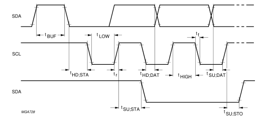
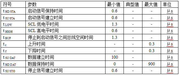
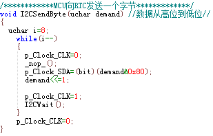
The problem with the above program is that the SDA data establishment time is too short. For some MCU with fast processing speed, data is sent out and RTC cannot respond. The correct approach is to set p_Block_CLK=1; Add a delay before:
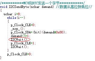
5. Device address error causing read/write register failure.
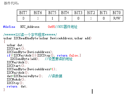
The above program is obviously an error in understanding the device address and is not familiar with the I2C bus operation process, and has not figured out the read and write operations of the device address.


