POP_UP_MESSAGE_CONTENT


Taken from Mastawei:Definition and measurement of jitter
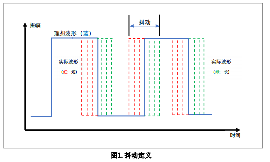
2. Shake type
There are various definitions of clock signal jitter, mainly including:
Period Jitter
Cycle to Cycle Period Jitter
Long Term Jitter
Phase jitter
Time Interval Error (TIE)
2.1 Periodic jitter
Periodic jitter is the deviation of the cycle time of a clock signal from a certain number of randomly selected ideal clock signal cycles.If we can measure a certain number of clock cycles, we can calculate the average time within the measurement window during this period Clock cycle and its standard deviation and peak to peak value. We usually refer to the standard deviation and peak to peak value as RMS value and Pk Pk, respectively Periodic jitter.
Peak to Peak Period Jitter = max(Tn) – min(Tn)
RMS Period Jitter = stdEV(Tn)
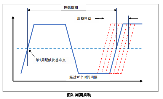
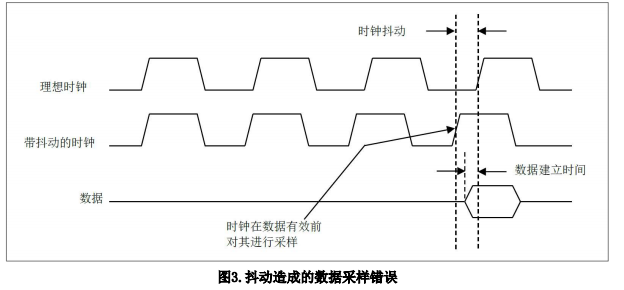
Periodic jitter is very practical for calculating temporal redundancy in digital systems. For example, in a microprocessor based system In the system, the processor requires 1 ns of data setup time before the clock rises. If the periodic jitter of the clock is -2.0 ns,The rising edge of the clock may occur before the data is valid, so the microprocessor may receive incorrect data.
The example is shown in the following figure.
2.2 Adjacent period jitter
Adjacent period (C2C) jitter, according to JEDEC standard 65B, is calculated by a certain number of adjacent period random samples Calculate the time variation of adjacent cycles. The JEDEC standard further stipulates that the size of each sample should be greater than or equal to 1000.It is worth noting that adjacent period jitter only involves the period difference between two consecutive periods and is independent of the ideal period.
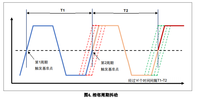
The adjacent period jitter is generally manifested as a peak value in ps, which is used to define the time difference between any two consecutive clock rising edges Maximum deviation. This type of jitter specification is commonly used to reflect the stability of spread spectrum clocks, as periodic jitter affects frequency spreading characteristics More sensitive, while adjacent period jitter is different.
2.3 Long term shaking
Long term jitter measurement refers to the change in clock signal edge and ideal position after multiple consecutive cycles. Used in actual measurements The number of cycles depends on different applications. Long term jitter is different from periodic jitter and adjacent periodic jitter, as it represents The cumulative effect of jitter on continuous clock cycle streams during long time intervals. Therefore, long-term shaking is sometimes referred to as fatigue Accumulated jitter. Long term jitter is often very practical for long-range telemetry applications such as graphic/video displays and rangefinders. Long-Term Jitter measures the jitter value of the clock edge after a considerable number of cycles (500-1000) lag from the reference point. The jitter parameter is also Clock stability is a very important indicator.
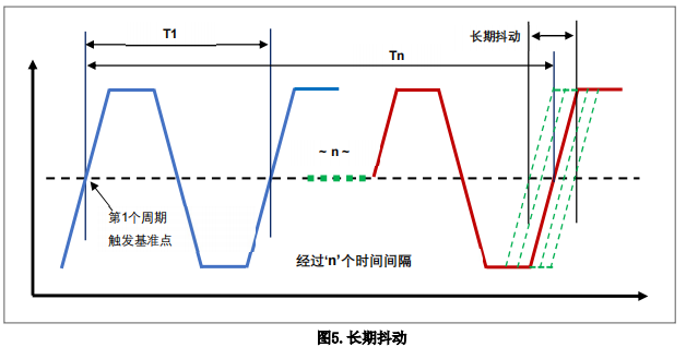
2.4 Phase jitter
Phase noise is described as the dBc/Hz value at a given frequency offset, also known as the noise spectral density value (e.g-70 dBc/Hz at 20KHz and -105 dBc/Hz at 10MHz, or a continuous curve within a frequency offset range Line diagram. Phase jitter is the integral of phase noise within a certain frequency offset range, expressed in seconds.
In the output square wave of the oscillator, most of the energy is located at the carrier frequency. However, some signal energy may 'leak into'On frequencies located near both sides of the carrier wave. Phase jitter refers to the phase difference between two offset frequencies relative to the carrier (fc)Total amount of noise energy.
2.5 Time Interval Error (TIE)
Time Interval Error (TIE) refers to the time point of the event edge of the actual signal relative to the time point of the event edge of the ideal signal The time deviation. TIE is the expression of the phase noise spectrum in the time domain discrete signal sequence, measured in seconds or ps. The following picture is
The basic concept of TIE.
The ideal signal is usually a reference signal obtained by signal processing software using an average estimation of the actual signal period.

3. Jitter testing method
3.1 Measurement cycle jitter
1. Measure the duration of one clock cycle (rising edge to rising edge)
2. Wait for a random number of clock cycles
3. Repeat the above steps 10000 times
4. Calculate the mean, standard deviation (σ), and peak to peak value based on these 10000 samples.
5. Repeat the above measurement 25 times. Calculate the average peak to peak value from these 25 results.
3.2 Measurement method for adjacent period jitter
1. Measure the cycle time of two adjacent clock cycles T1 and T2;
2. Calculate the values of T1-T2. Record the absolute value of this value;
3. Wait for a random number of clock cycles;
4. Repeat the above steps 1000 times;
5. Calculate the standard deviation (σ) and peak values for these 1000 samples. Peak value is the maximum absolute value in the data;
6. Repeat the above measurements 25 times and calculate the average peak value from these 25 sets of results.
3.3 Long term jitter testing method
1. Measure the time interval of 10000 consecutive clock cycles;
2. Wait for a random number of clock cycles;
3. Repeat the above steps 1000 times;
4. Calculate the mean, standard deviation (σ), and peak to peak values based on these 1000 samples.
5. Repeat the above measurement 25 times. Calculate the average peak to peak value from these 25 sets of results.
4. The harm of clock jitter to practical applications:
1. Increased data transmission error rate: Clock jitter can lead to an increase in data transmission error rate, especially in high-speed data transmission
In the middle. Jitter can cause dislocations, edge distortion, and temporal inconsistency, thereby affecting the accuracy and completeness of data.
2. Difficulty in system synchronization: Clock jitter can cause difficulties in clock synchronization and timing control for the system. When unstable
Clock signals may cause data loss, delay, and asynchrony, thereby affecting the overall performance of the system.
3. Difficulty in timing analysis: Clock jitter increases the complexity of timing analysis. In the presence of clock jitter, timing division
Analysis may require higher sampling rates and more precise measurement methods to accurately capture and analyze temporal relationships.
4. Design limitations: Clock jitter imposes limitations on system design. To avoid problems caused by jitter, system design needs to consider
Considering higher clock frequency tolerance, jitter compensation, and noise reduction increases design complexity and cost.
Conclusion:
Clock jitter is an important indicator for measuring the stability and accuracy of clock signals. It is responsible for data transmission, system synchronization, and timing division Analysis and design have a significant impact. Through methods such as frequency domain analysis, time domain measurement, phase interval measurement, and simulation, it is possible to Fully understand and evaluate the performance of clock jitter. A deep understanding of the definition, different types, and testing methods of clock jitter can help Optimize system design and ensure the reliability and accuracy of data transmission.


