POP_UP_MESSAGE_CONTENT


Basic knowledge of jitter and phase noise
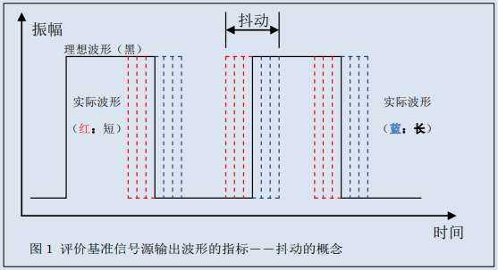
Figure 1 shows the situation where several cycles of signal waveforms appear in one cycle unit. The ideal waveform appears repeatedly in a single cycle, but a portion of the actual waveform's cycle becomes shorter (red) or longer (blue). Jitter is caused by extremely small instability in reading electronic signal components or adverse effects during signal transmission. Excessive jitter will cause mutual interference between adjacent signals, leading to degradation of image quality and sound quality when transmitting video and music signals. As mentioned above, jitter refers to the oscillation of a digital signal in the time domain, but the type of jitter is not limited to one. Jitter varies finely over time and has various patterns of temporal changes, making it difficult to evaluate jitter using a single parameter.
【2】 Explanation on the types of jitter
·Periodic jitter (peak to peak): refers to the jitter of the deviation amplitude (the difference between the maximum and minimum) in one cycle
·Standard deviation: The standard deviation indicating the degree of deviation
·Random jitter: Unpredictable jitter naturally occurring
·Deterministic jitter: jitter caused by factors such as circuits, electromagnetic induction, or external environment
·Accumulated jitter (long-term jitter): the continuous deviation of the clock in each cycle
Our company used the "DTS-2075" tester manufactured by Wavecrest during testing, and the testing conditions were to use a basically noise free power supply The probe test point is the output terminal, and the output resistance is set to 50 ohms.
The horizontal axis of Figure 2 represents one cycle (picoseconds), and in this test, a histogram is used to represent the period deviation of 50000 randomly selected samples. This is the data for SG-8002CA125MHZPCB. The ideal scenario is for a peak to appear at one cycle of 125MHz, but the characteristics may change due to various factors. PLL is particularly prone to the tendency shown in the right figure, so it is important to understand this characteristic correctly and reflect it in the design.
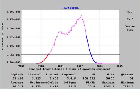
Figure 2: Histogram of data
1) Periodic jitter (peak to peak jitter) is the amplitude of the deviation displayed in the periodic jitter. Our company uses peak to peak values to represent this deviation. The difference between the longest and shortest periods in the above figure is the peak to peak jitter.
2) Standard deviation jitter (1 standard deviation)
The standard deviation jitter is the standard deviation (1) obtained from the above test results. From this, it can be concluded that the probability of occurrence in 12.5ps is 68.26%. However, peak to peak jitter only displays a very small portion of the state (a few milliseconds) of quartz products that are usually used for a long time, and cannot display the overall jitter; The standard deviation jitter is only effective under the ideal normal distribution (also known as Gaussian distribution), and the reliability of the values is very low under other distributions. For this purpose, an analysis method was established to divide the histogram obtained from the test into two components in order to capture the overall state of jitter.
(3) Random jitter (RJ)
Random jitter represents unpredictable jitter components, truly deserving of its name. It is naturally generated due to the characteristics of the components themselves, thermal noise, and other factors. Therefore, an ideal normal distribution is set in the histogram, and the histogram obtained from actual shaking testing is used to predict based on the curve fitting of the rising and falling boundaries of the curve. Moreover, random jitter is represented by standard deviation: often using the expressions of "RJ on the left" or "R on the right".
(4) Deterministic jitter (DJ).
Deterministic jitter is caused by circuit design, electromagnetic induction, or external factors. In actual test results, it can be represented by the part sandwiched between the left and right random jitter. By summarizing the above viewpoints on jitter, it can be concluded that the jitter components in a cycle are composed of both naturally occurring random jitter and deterministic jitter caused by human factors.
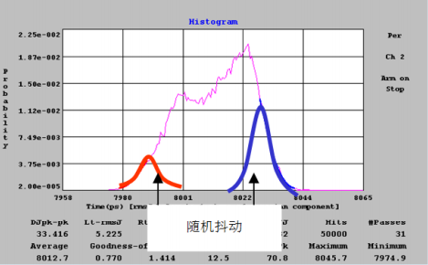
Figure 3: Explanation of Random Jitter
Reducing jitter is equivalent to minimizing deterministic jitter as much as possible. Optimizing the components of deterministic jitter can make the left and right random jitter coincide with each other, achieving an ideal normal distribution.
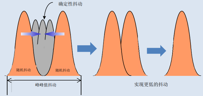
Figure 4: Explanation of deterministic jitter
(5) Accumulated jitter (long-term jitter)
The jitter described above has been tested for deviation based on one cycle, but some jitter cannot be expressed solely based on this. This is cumulative jitter.
Accumulated jitter not only represents the deviation of one cycle, but also represents the deviation of multi cycle continuous waveforms such as two cycles and three cycles, as shown in the chart on the right.
The horizontal axis of the chart represents the number of testing cycles, and the vertical axis represents 1 standard deviation for each cycle. Observing the accumulated jitter can confirm the duration of several cycles of jitter The state of change in motion. The jitter accumulated over a period tends to contract by 1 standard deviation from a certain period. We can use this to determine the performance of the PLL circuit
Bandwidth and over response characteristics.
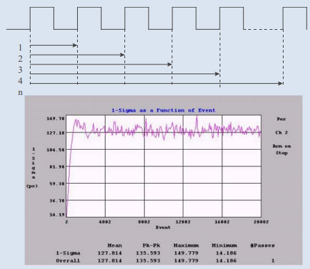
Figure 5: Explanation on Accumulated Jitter
【3】 The relationship between oscillator output and jitter
Quartz oscillators not only output the frequency at which they should vibrate, but also output frequency components.
From the frequency characteristics of the output signal of the quartz oscillator shown in Figure 6, it can be seen that there are "skirts" of other frequencies around the fundamental frequency. This is phase modulation caused by random signals, which is generated by modulating oscillators with noise sources and is commonly referred to as "phase noise". These frequencies are mostly higher than the background noise and appear near the carrier frequency. Noise can be expressed using the following formula:
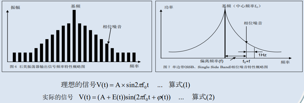
Here, E (t) represents the change in amplitude (amplitude noise), and φ (t) represents the change in phase (phase noise). φ (t) is phase noise.Phase noise is usually defined as the ratio of the noise power deviating from the carrier frequency to the carrier power. All phase noise becomes jitter.In general, the phase noise is represented by "Single Side Band (SSB) phase noise L (f)". L (f) is the deviation from frequency The function of f is in dBc/Hz. The single sideband power caused by phase change is defined as the total power of an electrical signal with a bandwidth of 1Hz deviating from the carrier frequency fHz (Figure 7), which can be expressed by the following equation:

L (f) is noise, so it must be converted to 1Hz units for comparison. If the measured frequency bandwidth for testing phase noise is set to A, L (f) can be calculated by dividing the phase noise obtained from the test by A. For example, if the test bandwidth is 1kHz and the test result is -70dBc, conclusions can be drawn of -70dBc, -30dB, and -100dBc/Hz. 1Hz is 1/1000 of 1kHz, so the average output of the bandwidth is also 1/1000 (=-30dB). DBc/Hz is the standard unit for representing phase noise.
Phase noise is not only generated in quartz oscillator circuits, but also in PLL circuits due to noise originating from various circuit components, noise components, or loop characteristics. Phase noise refers to the oscillation of signal phase. Therefore, by observing the temporal changes, the waveform jitter previously described can be seen.
【4】 Phase jitter
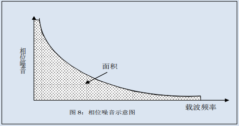
Along with jitter, it represents the stability of the signal and is interrelated. Specifically, phase noise manifests as frequency instability in the frequency domain, while jitter represents the oscillation of signal waveforms in the time domain. As mentioned earlier, the horizontal axis represents deviation frequency and the vertical axis represents phase noise. The integral value of the phase noise (represented by the dot in Figure 8) belongs to the phase jitter of random jitter.
By calculating the integral of a specific deviation frequency range, the phase jitter value with specific frequency range components can be obtained.
The market requires quartz components to have various application characteristics. Including the characteristics of jitter and noise previously introduced, Epson will continuously provide quartz component products that meet customer needs.
