1. Introduction
Differential clocks are widely used to achieve high-speed, noise-tolerant clock transmission. Clock manufacturers
including Epson offer differential clock products in a variety of formats, and it is necessary to make the appropriate
selection according to the requirements of the system. Epson has offered differential clock products in three
standard formats: LV-PECL, LVDS, and HCSL, and now we have newly added our proprietary Wide-Amplitude
LVDS, or WA-LVDS, to the lineup. This technical note explains the characteristics of these four differential clocks.
2. Overview of differential clocks
① LV-PECL
LV-PECL stands for “Low Voltage Positive Emitter Coupled Logic”. As you can see from the word "Emitter", it is an output driver composed of bipolar transistors. Since ECL which is a root of LV-PECL required a negative power supply, the word "Positive" was added to emphasize that the driver operates with a positive power supply. The word “Low Voltage” is further added after a product which operates with a power supply voltage of 3.3 V came out.Nowadays, since products operable with 3.3 V or lower became quite general, "LV-" is often omitted.
LV-PECL is suitable for high-speed operation because the output transistors operate without being shut off, as explained later. In addition, since the amplitude is relatively large, low phase noise feature is available, as well as excellent noise immunity.
② LVDS
LVDS stands for “Low Voltage Differential Signaling”. As the name suggests, LVDS is characterized by its low amplitude operation. LVDS was first developed mainly by National Semiconductor (later acquired by Texas Instruments). It was then standardized by ANSI/TIA/EIA in 1994 and is currently used in quite many electronic devices.
The most general amplitude level is 0.35 V (Typ.). By keeping the amplitude low, high-speed operation with low driver current is achieved. Low current consumption is a major advantage of LVDS. However, due to the low amplitude, its phase noise tends to deteriorate. In addition, it must be noted that the receiver needs a considerable amount of power to expand the amplitude to the desired level, and phase noise might be degraded during this process。
③ HCSL
HCSL stands for “High-speed Current Steering Logic”. This name comes from the circuit structure that the current output path is steered alternately between positive and negative output terminals. This method was proposed in the PCI-Express standard, and it is still a major application today. The output waveform of the HCSL driver provided by Epson is adjusted so that the edged rate is appropriate or not too steep. This is because the clock frequency used for PCI-Express is 100 MHz in usual, and the edge rate is required to be fitted for that frequency.Therefore, although the amplitude level is almost the same as LV-PECL, the phase noise is somewhat disadvantageous compared to it.
④ WA-LVDS
In recent years, clock receivers on ASICs and SOCs have become more customized, so the standard differential clocks mentioned above are not always suitable. Therefore, Epson recently released Wide-Amplitude LVDS, or WA-LVDS, to provide a differential clock that provides superior performance and flexibility.
WA-LVDS maintains the simplicity of the LVDS load connection, and provides flexibility to the offset voltage and signal amplitude. The offset voltage level and amplitude can be selected from four levels and ten levels,respectively (details will be described later). Therefore, in many cases, you can connect the clock directly to your LSI without the need for extra components. Of course, AC coupling with capacitors is also possible. If you choose large amplitude, current consumption increases but lower phase noise is expected. WA-LVDS is applicable for both systems which are oriented in low consumption and low noise. Another advantage of WA-LVDS is that it has higher PSNR (Power Supply Noise Rejection) performance than LVDS.
3. Classification of differential clocks
Although it is not well recognized widely, differential clocks are broadly divided into two types: current output type and voltage output type. The current output type obtains the desired output amplitude by passing a specified current through the load resistor. Thus, the amplitude also depends on the accuracy of the load resistance. On the other hand, the voltage output type directly outputs a specified voltage to the load. The amplitude is not very dependent on the accuracy of the load resistance.
Furthermore, when classified from the perspective of the current flowing through the load resistance, the current can be divided into two types: pure AC and AC + DC. Inevitably, clock drivers that include a DC component require an excess current consumption.
Based on these combinations, differential clocks can be classified into four types which are shown in Table 1. The newly developed WA-LVDS is a voltage output type, and the current flowing through the load resistance is pure AC. This is exactly an ideal combination for a differential clock.

Note 1: Some products have a pseudo-realization of LV-PECL as a current output type.
Note 2: LP-HCSL (Low-Power HCSL) which is proprietary to Renesas (formerly IDT) is a kind of HCSL,
but it belongs to the same classification as LV-PECL.
4. Output voltage and current
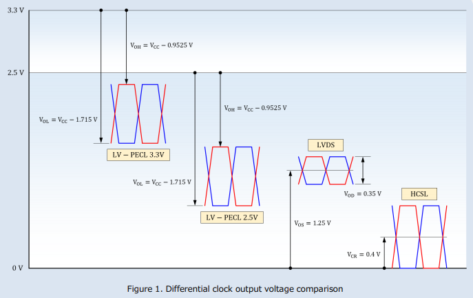
Let's look at the differences in output voltage for the three existing clocks, i.e., LV-PECL, LVDS, HCSL. Please refer to Figure 1.
The most unique one may be LV-PECL. The output voltage of LV-PECL is defined with respect to the supply voltage VCC. Therefore, the output voltage value changes depending on the supply voltage. Specifications of the H level output voltage VOH and L level output voltage VOL are shown in the figure. The differential amplitude is 0.7625 V(Typ.) regardless of VCC.
For LVDS, the offset voltage VOS is specified as 1.25 V and is independent of the supply voltage. The differential amplitude VOD is 0.35 V, which is significantly the smallest value among the three methods.
The last one, HCSL is characterized by the L level being 0 V. The specification usually determines a differential crossing point voltage VCR of 0.4 V. There are often no clear regulations regarding the H level. But inevitably, it is designed around 0.8 V. Hence, the amplitude level is approximately the same as LV-PECL.

Next, let's look at the output current. The output current here means the current that flows from the driver’s output terminals to the load (or flows in from the load) which forms the output voltage indicated in Figure 1. Please refer to Figure 2.


