POP_UP_MESSAGE_CONTENT


Epson Announces the Development of Unique Wide-Amplitude LVDS Output - Flexibly selectable low-noise output matched to the LS -
Seiko Epson Corporation (TSE: 6724, "Epson") has developed a new differential output* scheme for crystal oscillators. The new scheme, wide amplitude low-voltage differential signaling (WA-LVDS), enables flexible selection of the output best suited to the amplitude level required by an LSI. Epson plans to have crystal oscillators with WA-LVDS output commercially available in the 2025 fiscal year (starting April 2025).
Data traffic is rapidly growing along with recent advances in digitalization, and 5th-generation mobile telecommunications systems (5G), the Internet of Things (IoT), and next-generation communication systems will need faster transmission speeds and higher capacities to support this traffic. General-purpose differential outputs such as LVDS, LV-PECL, and HCSL are required for data transmission in such systems. Each of these schemes have their own characteristics, and engineers select the best one for their particular system. In recent years, however, the higher performance required of communication equipment has meant that circuits are now being engineered to receive the optimal differential output for LSIs used in communication equipment. As a result, general-purpose differential output cannot be used in a growing number of cases. Accordingly, the demand for differential outputs suitable for LSIs is expected to grow even stronger in the future.
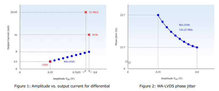
Existing LVDS with general-purpose differential output has lower current consumption than LV-PECL and HCSL. On the other hand, however, it also has lower amplitude and thus less noise immunity. To address this issue, Epson developed WA-LVDS, a differential output with selectable amplitude levels that can be used flexibly. WA-LVDS increases noise immunity by making it possible to easily obtain high amplitude. It also offers lower current consumption than LV-PECL and HCSL.
As a leader in crystal devices, Epson will continue to provide crystal device products that meet the needs of all manner of electronic devices and social infrastructure.
*: Differential output is a signaling method in which data is transmitted as the voltage difference between two separate lines of opposite polarities. Advantages of differential output include high-frequency data transmission and high noise immunity.

*: Phase jitter: Fluctuation of the clock period is called jitter. Phase jitter is a measure of edge deviation from a jitterfree ideal clock and can be calculated from the phase noise characteristic


