POP_UP_MESSAGE_CONTENT


EPSON S2D13P04 is suitable for multi camera interface ICs
S2D13P04, The Epson camera interface IC is suitable for multi camera systems. 4 camera inputs and 4 mode outputs; Fixed channels, merging, automatic scanning, and compression. Due to the built-in VRAM for image processing, a 4into1 camera interface can be implemented through a microcontroller. It is easy to increase the number of cameras without any changes from one camera system.
S2D13P04 Description
S2D13P04 is a camera interface IC designed specifically for automotive multi camera systems.
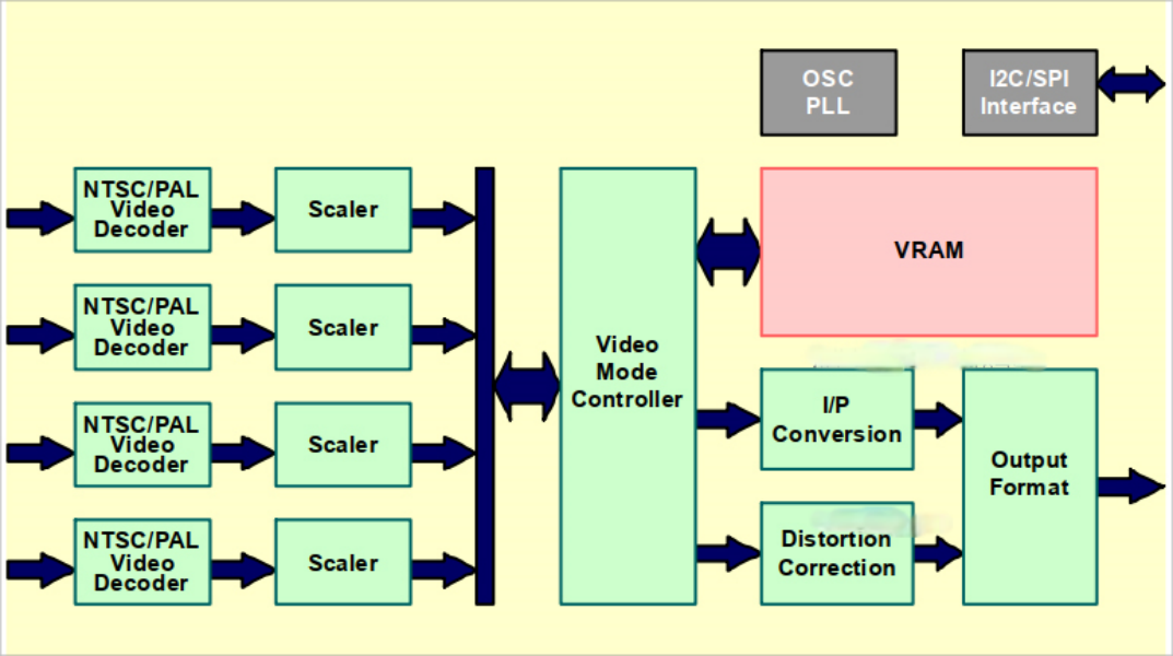
S2D13P04 integrates four NTSC/PAL video decoders, which can simultaneously connect four analog cameras and synchronously output asynchronous input image data from the four cameras through internal VRAM.
S2D13P04 also has image processing functions, such as image synthesis of four camera image data, distortion correction, and conversion from interlaced scanning to progressive scanning.
S2D13P04 has a large capacity VRAM built-in, so no external memory is required.
S2D13P04 features
l Video input
Analog Video (CVBS) Input -4 inputs
PAL/NTSC decoder -4 channels
NTSC-M and NTSC-J support
PAL-M, PAL-B, PAL-G, PAL-I, PAL-N support
l Video output
Digital output 8-bit YUV422 (with HSYNC/VSYNC) ITU-R BT.656 * 1
Interleaved output * 2, 3
Progressive output
l Video output mode
Fixed mode
Automatic scanning mode * 4
Merge Mode * 2
Compression mode * 2, 4
l image processing
Image scaling function
Interleave to inline conversion
Distortion correction function * 3, 4
l Output at a stable frame rate
720x480i 30fps (NTSC interlaced output)
640x480p 30fps (NTSC output line by line)
640x480p 30fps (NTSC with distortion correction enabled)
720x576i 25fps (PAL interlaced output)
768x576p 25fps (PAL output line by line)
640x480p 25fps (PAL with distortion correction enabled)
l Host interface
I2C interface (slave)
SPI interface (slave)
l No external RAM required
l Working temperature -40 to+85 ℃ (Ta)
l Working voltage simulation: 3.3 ± 0.3V, IO: 3.3 ± 0.3V, Core: 1.8 ± 0.15V, PLL: 1.8 ± 0.15V z
l encapsulation
S2D13P04B00B100 PFBGA10UX121 (10mm×10mm×1.2mm, 0.8mm-pitch)
S2D13P04F00A100 QFP15-100pin (14mm×14mm×1.7mm, 0.5mm-pitch)
*The number of pixels per row may not comply with the ITU-R BT.656 standard.
*In merge mode or compression mode, the output is compatible with interlaced output.
*When the distortion correction function is enabled, interlaced output is not supported.
*In compression mode or automatic scanning mode, distortion correction is not supported.
S2D13P04 System Block Diagram


