POP_UP_MESSAGE_CONTENT


Performance requirements for reference clocks related to 5G communication
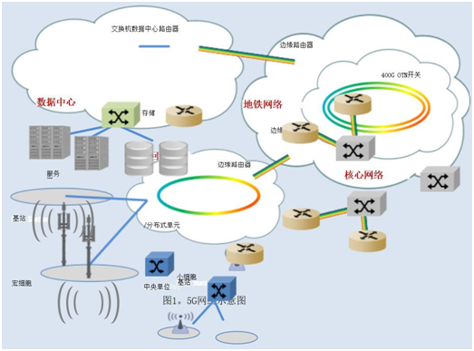
Optical network market
The core network connecting 5G base stations and data centers, as well as the subway network, is composed of a
A fiber optic network connected by optical fibers. With the deployment of 5G, optical transmission
Efficient and high-capacity communication technology has been developed and invested in
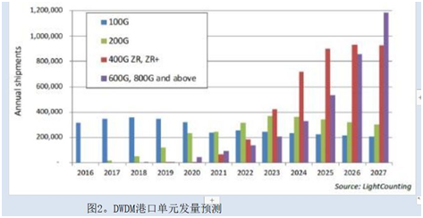
Actual use. In addition, the links between data centers, also known as Data Center Interconnection (DCI), are utilizing 100G, 200G, and 400G connections, as well as 400G coherent DWDM (dense wavelength)
The division multiplexing interface 400ZR has been standardized, and 800ZR is currently under development.
The 400GbE using PAM4 has been standardized, and the release of 100G PAM-4 PHY with a speed of 800 Gbps has begun
Client transmission and. Figure 2 shows the shipment volume of DWDM port units, including 400ZR and
800G. In the future, with the popularization of 5G, 400ZR, 800ZR, and PAM4 are expected to enter the optical network market.
5G base station market
In order to increase network capacity, it is also necessary to increase the data throughput of the base station. this
The technology that contributes the most to increasing the capacity of 5G wireless networks is the expansion of frequency bandwidth. Now frequency bandwidth can be extended by using carrier frequencies higher than LTE. The maximum frequency bandwidth of LTE per channel is 20 MHz, but with the 3GPP version 15,5G, the maximum frequency bandwidth has been extended to 100MHz for FR1 (carrier frequency: 410 MHz to 7125MHz) and 400MHz for FR2 (carrier frequency: 24.25 GHz to 52.6 GHz). As shown in Figure 3, the total shipment volume trend of the base station market is stable, but due to the switch to LTE, it is expected that the shipment volume of 5G base stations will increase.
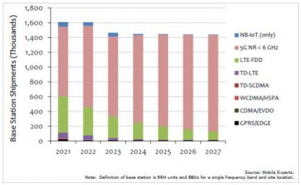
Figure 3. Base Station Market Forecast
Specification for communication system and reference clock requirements for 5G PAM4
In history, NRZ transmission using on/off key control has been widely used in optics
Communication is due to their simplicity. Recently, a pulse amplitude modulation technology,
PAM4 has been adopted, which encodes two bits simultaneously using multiple amplitude levels. This makes it possible to safely transmit at twice the speed as NRZ.
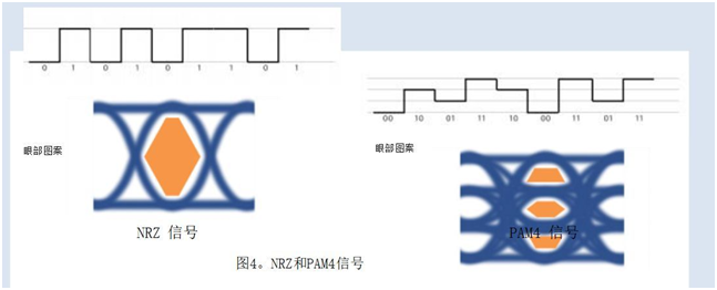
Compared to the NRZ (non regression to zero) signal, the PAM4 signal has a smaller eye opening
The orange part in the picture shows that the quality of the transmitted signal tends to deteriorate when observed in eye mode. To ensure the quality of the transmitted signal, there is an SPXO (simple packaging)
A crystal oscillator with low jitter performance is required as a reference clock. Approximately 100 fs is
As an effective threshold for the reference clock. In addition, due to the modularity of the optical communication unit, the reference clock must be very small and consume low current.
400ZR
400ZR uses coherent optical transmission technology to achieve speeds of up to 400 Gbps over long distances. Unlike NRZ or PAM4, 400ZR uses orthogonal modulation, performed by numbers
Coherent signal processing circuit, where modulated data is transmitted over coherent light.
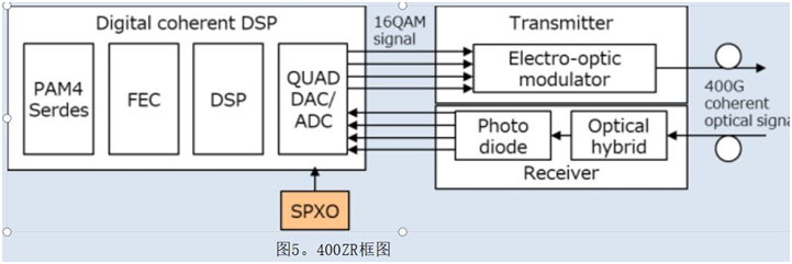
To process a 400G signal, the sampling clock required for the DAC/ADC processed by this signal
The circuit requires an SPXO with frequencies typically between 156.25 MHz and 500 MHz, and low jitter characteristics of approximately 100 fs. In addition, the frequency tolerance is specified by OIF-400ZR -01.0, and an accuracy of ± 20 x 10-6 is necessary. The entire system requires low power consumption and has a strong preference for clocks with low current consumption characteristics.
5G wireless base station, RU (radio unit)
In 5G wireless base stations, complex technologies such as QAM (Orthogonal Amplitude Modulation) and OFDM (Orthogonal) are used
Frequency division multiplexing (FDM) to maximize throughput
Given wireless spectrum channel.
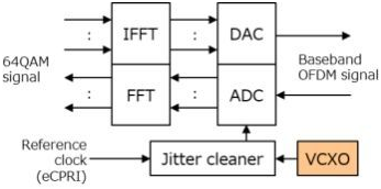
Figure 6. OFDM Block Diagram
With the accelerated transmission speed due to the expansion of frequency bandwidth, DAC/ADC in OFDM 5G systems require faster and more accurate sampling clocks than LTE. Therefore, VCXOs
The jitter cleaner for voltage controlled crystal oscillators requires high frequency and low jitter
In recent years, the technology of using SPXO as a jitter reference clock has been developed
The cleaning agent has gradually entered the practical use stage. However, even so, SPXOs must have a higher frequency
And low jitter characteristics. In addition, as the base station is installed outdoors
Exposure to vibrations in the surrounding environment requires a clock with stable characteristics when exposed to vibrations; That is to say, clocks with low acceleration sensitivity
Implementation Technology of High Frequency Clock
SPXO or VCXO are typically used for high-frequency clocks of 100 MHz or higher, and their configuration allows the oscillator and integrated circuit to be built into one package. There are several types of
The technology for implementing high-frequency clocks. These technologies are integrated with built-in crystal units or integrated circuits. Here, the technology and characteristics of implementing high-frequency clocks are
Show me
-Fundamental mode oscillator: high-frequency crystal unit+fundamental mode oscillator circuit (IC)
In a regular quartz crystal unit, quartz is cut out at a so-called AT cutting angle
Process into a thin crystal chip based on frequency. The higher the frequency, the thinner the frequency that needs to be processed. The thickness of a 100-MHz crystal unit is 16.7 μ M. Stable high
By combining crystal units with high-frequency oscillator circuits, a frequency clock with low noise and low jitter can be obtained. On the other hand, due to the thinness of the crystal chip, its content is also very low
Mechanical strength is high and susceptible to vibration.
-Third overtone mode oscillator: Third overtone mode crystal unit+Third overtone oscillator circuit (IC) In addition to fundamental mode vibration, the crystal unit also has other odd harmonics, such as the third and fifth harmonics. The third harmonic crystal unit resonates in the third harmonic mode. In other words, a 100mHz third overtone mode crystal unit has the same thickness (50.1 μ M)
33.3333 MHz crystal unit. This relatively large thickness increases the mechanical strength and makes the crystal less susceptible to vibration damage. It also has low noise and jitter
Characteristics equivalent to fundamental mode oscillators. However, the equivalent series resistance at the third harmonic is relatively high, which increases the difficulty of designing oscillation circuits,
The fundamental wave oscillates according to changes in the working environment, which may cause fatal problems during system operation.
Due to the high Q value, the frequency is also not high
Even if the load capacitance of the oscillation circuit is changed, it is easy to change, so VCXO is not suitable.
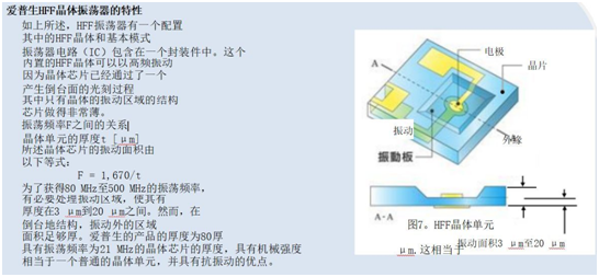
-HFF (high-frequency fundamental oscillator) oscillator: HFF crystal unit+fundamental oscillator circuit (IC)
HFF crystal oscillators can vibrate at high frequencies because they have an inverted top film structure, which is achieved by using photolithography to only etch the vibration region of the crystal chip to an extremely thin layer. Due to the sufficient thickness of the crystal chip in the outer area
Vibration area, with high mechanical strength and resistance to vibration. Combining crystal units with high jitter can achieve a stable high-frequency clock with low noise and low jitter
Frequency oscillator circuit.
-PLL oscillator: low-frequency crystal unit+baseline oscillation circuit and PLL circuit (IC)
The PLL oscillator uses a low-frequency crystal unit that is resistant to mechanical stress and vibration as the crystal unit. Multiply the frequency obtained from the oscillation circuit by the PLL circuit to obtain a higher frequency. Although PLL circuits can relatively easily generate high-frequency clocks, they increase noise, so their jitter characteristics are not as good as other technologies. As the PLL circuit is driven, the current consumption tends to increase.
MEMS (Micro Electro Mechanical Systems) oscillators use MEMS resonators instead of quartz crystal resonators.
-SAW (surface acoustic wave) oscillator: SAW resonator+basic oscillation circuit (IC)
Surface acoustic wave resonator is a device that generates surface acoustic waves on the surface of a crystal chip and resonates with the crystal chip. The characteristics of surface acoustic wave resonators are not determined by thickness
The crystal chip, but the distance between the comb shaped electrodes (between digits)
Sensor (IDT) is formed on the surface of the crystal. The frequency can be increased to approximately 1 GHz
By using photolithography technology to form electrodes and produce thicker crystal chips
And it has high mechanical strength. The noise during oscillation is also very low and can achieve lower jitter characteristics. On the other hand, the frequency/temperature coefficient of the crystal
The unit has third-order characteristics, while the wave resonator has second-order characteristics, resulting in lower frequency stability.
Tabu e1 summarizes the high-frequency technologies and their characteristics mentioned above.
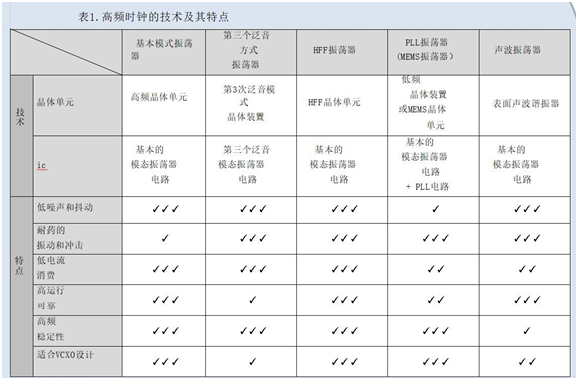
Regarding various technologies available, Seiko Epson has chosen to use HFF oscillators
A successful system will commercialize high-frequency clocks that meet the needs of the 5G communication market.
Impact and vibration performance
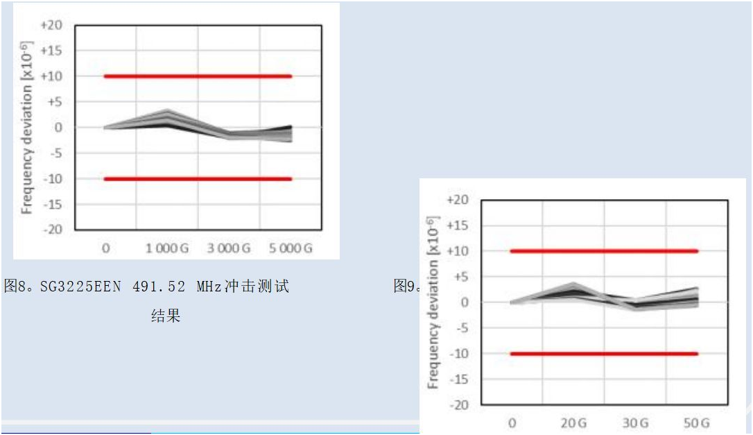
Our product undergoes impact and vibration testing during reliability testing. Below image
The impact and vibration test results of our 491.52-MHz HFF SPXO SG3225EEN are displayed. It passed the internal standard of ± 10 ppm frequency fluctuation. Under standard conditions
Impact test 1000g, vibration test 20g. Furthermore, even if vibrations and impacts exceeding the standard conditions were applied, there were no malfunctions caused by HFF
The oscillator is damaged with no abnormal frequency fluctuations. This result proves that HFF oscillators have high impact and vibration performance at the upper limit of 500 MHz.
-Acceleration sensitivity (G sensitivity)
As mentioned earlier, due to the installation of base stations outdoors, they are exposed there
The vibration in the surrounding environment requires a clock with minimal frequency variation when exposed to vibration, that is, a clock with low acceleration sensitivity. At Epson, crystal chips
The shape with the least impact on the characteristics during vibration was simulated through eigenvalues
And analysis was conducted, and optimized design was verified through experiments. The following figure shows the G sensitivity of Epson 122.88-MHz HFF VCXO VG7050VFN. The low acceleration sensitivity of 2 x 10⁻⁹/g has been achieved.
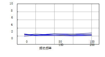
Figure 10. 122.88-MHz VG7050VFN G sensitivity
-Frequency/temperature coefficient
For 400ZR, a clock frequency tolerance of ± 20 x 10-6 is necessary. This is impossible to achieve with a crystal oscillator, as the frequency/temperature coefficient alone exceeds ±
20 x 10-6 between -40 ° C and+85 ° C. Epson's HFF SPXO SG2520VHN provides these features
As shown in the figure below, Epson has already added a temperature compensation circuit to the integrated circuit. This meets the requirements of 400ZR.
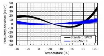
Figure 11. Frequency/Temperature Coefficients of Ordinary Crystal Oscillator and SG2520VHN
Phase noise, phase jitter, PSNR (power noise suppression) characteristics
Epson's HFF oscillator uses an HFF crystal unit to achieve stable high-frequency oscillations of up to 500 MHz with low noise and low jitter. In addition, the built-in Epson IC has a carefully considered low-
Optimized noise design was carried out through simulation. The following figure shows the phase noise characteristics of Epson's 491.52-MHz HFF SPXO SG2520VHN and 491.52-MHz HFF VCXO
VG3225VFN. Both have good phase noise and phase jitter characteristics.

In practical applications, the power supply voltage applied to the oscillator contains noise, which can lead to the deterioration of the oscillator's phase noise and phase jitter characteristics. in order to
For example, when the power supply voltage contains noise with a frequency component of 10 kHz, spikes are spurious and occur near the offset frequency of the phase noise
Epson's HFF SPXO features a low-noise LDO (low loss) that can stabilize power supply voltage, reduce noise, and limit the deterioration of phase noise and phase jitter
The characteristic diagram shows the phase jitter characteristic, i.e. PSNR
When noise is superimposed on the power supply voltage of SG2520EHN and an
Equivalent products from competitors. The noise model is a sine wave with a frequency of 20
From kHz to 5 MHz, the horizontal range is 50 mVp-p. It can be confirmed that the deterioration of the phase jitter characteristics of SG2520EHN is limited.
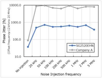
Figure 14. PSNR characteristics of SG2520EHN and its competitor products
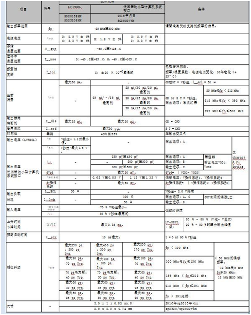
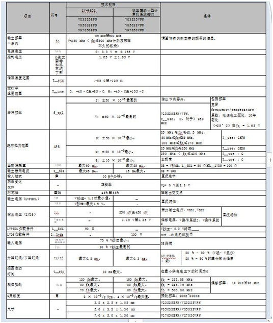
Detailed specifications for Epson HFF oscillators
The detailed specifications of our HFF oscillator (SPXO/VCXO), characterized by
Meet the needs of the 5G communication system market, as shown in the following figure.
-HFF SPXO: SG2016EHN/SG2520EHN, SG2016VHN/SG2520VHN specifications.
Detailed information about the above products can be found on our website.
specifications
Detailed information about the above products can be found on our website.
conclusion
The HFF oscillator is the best reference clock for 5G communication systems, helping to maximize the value of customer products.
Seiko Epson will continue to recommend crystal equipment that can enrich social wealth.


