POP_UP_MESSAGE_CONTENT


Notes on the Use of RA8900CE Clock Chip

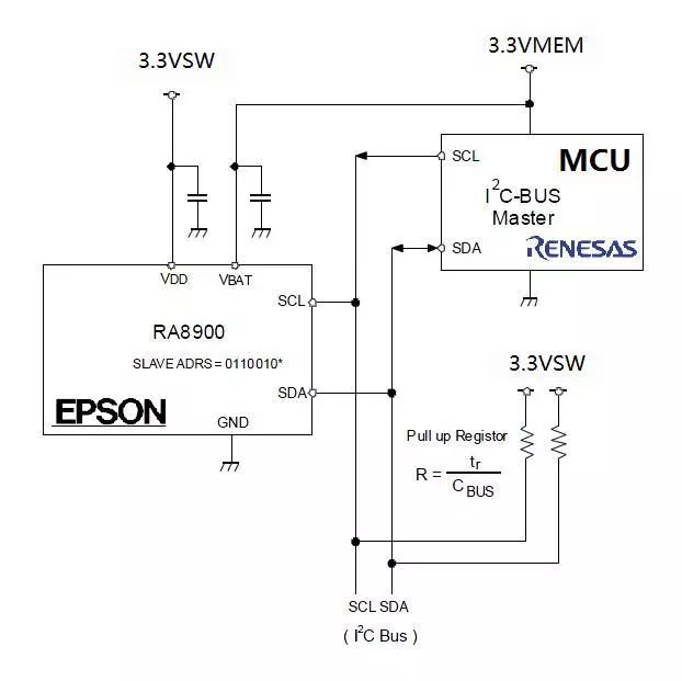
Figure 1: Clock display circuit diagram of car display screen
Problem analysis and resolution
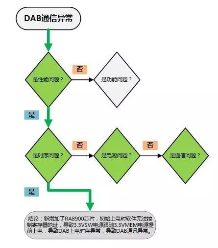
The sample is powered on for the first time, and the DAB chip cannot communicate with the MCU normally. This is a challenging question, and in order to explore the reasons, we adopt an exclusion method of thinking and analyze it as follows:

Figure 2: Problem Analysis
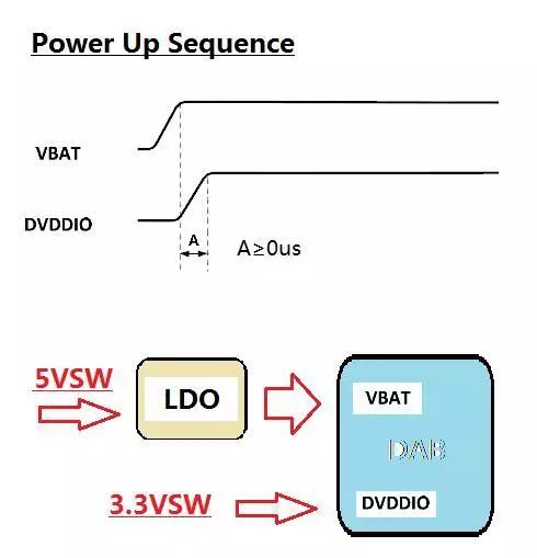
Firstly, lock the module that caused the problem. We first confirm the power on timing of the DAB, as shown in Figure 3. The DAB chip has a requirement for the power on timing, that is, the interface power supply DVDDIO must be powered on after the main power supply VBAT. However, after testing, we found that DVDDIO was powered on earlier than VBAT, resulting in abnormal DAB communication. The cause of DAB communication abnormalities has been identified, but why is the power on timing not met?
The DAB power supply we designed is shown in Figure 3, which controls 5VSW and 3.3VSW through MCU to ensure that 5VSW and 3.3VSW are powered on in advance. The theoretical design fully meets the requirements of DAB power on timing. But why is there a significant difference between the actual situation and the theoretical design?

Figure 3: DAB power on timing
By measuring the power supply timing, we ultimately found that it was due to the addition of the RA8900CE chip, which caused power supply cascading during the initial power on stage. The 3.3VSW power supply followed the 3.3VMEM to power on earlier, resulting in non-compliance with the DAB power on timing requirements.
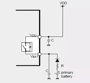
The internal circuit of RA8900CE is shown in Figure 4. In order to prevent power failure during 3.3VSW, we set the register address of RA8900 to VDETOFF, SWOFF=(1.1). This setting ensures that the switch between the VDD and VBAT inside RA8900CE is always turned off. But when the machine is first powered on, the register of RA8900CE is set to the default value, and our software can only set the register address of RA8900CE to VDETOFF after the MCU is up SWOFF=(1.1). This will result in a period of time when VBAT and VDD are directly connected, causing the 3.3VSW power supply to follow the 3.3VMEM to power on earlier, leading to abnormal communication between DAB and MCU.

Figure 4: Internal circuit of RA8900CE
Knowing the root cause of the problem makes it easy to find a solution. Due to the maximum current consumed by the VDD power supply during RA8900CE operation being 1.45uA, the current consumption is very small. Therefore, we have decided to adopt the solution of sharing the same power supply for VDD and VBAT, that is, using a 3.3VMEM power supply for both. This fundamentally solves the problem of serial power supply, thereby ensuring the power on timing of DAB and solving the problem of communication failure between DAB and MCU.


