POP_UP_MESSAGE_CONTENT


The real-time clock module RX8901CE has a digital temperature compensation function, helping industrial equipment achieve precise control
In the field of industrial control, electronic products have a wide range of operating temperatures, and the same product will face different working conditions such as high and low temperatures. For circuit designs that are sensitive to clock signals, temperature changes will seriously affect product functionality. Therefore, high-precision clocks are needed to ensure the stability of circuit signals. In this case, real-time clock modules with digital temperature compensation characteristics are needed to complete the design. The real-time clock module completes clock signal interaction through a digital signal interface, converts temperature related analog signals into digital signals within the module based on temperature changes, and finally communicates with the digital interface of the computing circuit to complete the clock function.

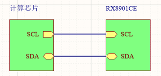
Figure 1. Circuit connection of digital temperature compensation for I2C interface
RX8901CE is a real-time clock module with digital temperature compensation features launched by EPSON company. This product has an IC digital interface and can achieve high-precision temperature compensation through interaction with digital chips, suitable for circuit structures with multiple computing chips.

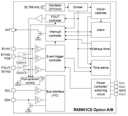
Figure 2 Internal structure diagram of RX8901CE
Support IC digital interface to achieve clock signal transmission between multi chip circuits
The RX8901CE clock module uses the I2C bus to exchange data with external chips, and the communication frequency can reach 400kHz in a fast manner. The 12C bus adopts a bidirectional and half duplex serial communication protocol, which can be implemented using two hard wires: clock (SCL) and data (SDA), and can communicate with multiple digital chips simultaneously. Especially suitable for achieving real-time clock signal synchronization among multiple chips in the same circuit system, such as MCU, FPGA, etc., ensuring the synchronization of circuit clock signals

Figure 3 Frequency characteristics of RX8901CE
Stable frequency characteristics, suitable for use in environments ranging from -40 ℃ to+105 ℃
RX8901CE is divided into two different models, XS and XB, based on its frequency characteristics. From the frequency characteristic table in Figure 3, it can be seen that the RX8901CE XS model product has a frequency tolerance of ± 3.0x10⁻⁶ in a temperature environment of -40 ℃~+85 ℃, and RX8901CE XB has a frequency tolerance of ± 5.0x10⁻⁶ in the same temperature environment. The frequency characteristic of the product shows excellent performance in environmental temperature changes, meeting the high-precision temperature compensation requirements in industrial environments. At the same time, in the working environment of+85 ℃~+105 ℃, the frequency tolerance of the product has decreased, but it still provides stable working parameters for designers to refer to.

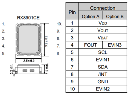
Figure 4 Pin distribution of RX8901CE
The module pins have rich functions and provide multiple input and output functions
RX8901CE provides 10 pins, including 3 event input pins, frequency output pins, and interrupt output pins. The frequency output pin is multiplexed with one event input pin. For event input pins, the status configuration of the clock module is mainly achieved through external pull-up and pull-down resistors. The frequency output pin is used to control the working frequency of the clock module, and the output of 32.768KHz, 1024Hz, and 1Hz can be set through relevant configuration operations. The interrupt output pins provide various interrupt functions such as clock wake-up, alarm, and event detection for the external system, allowing the computing chip to grasp the real-time status of the clock module.


