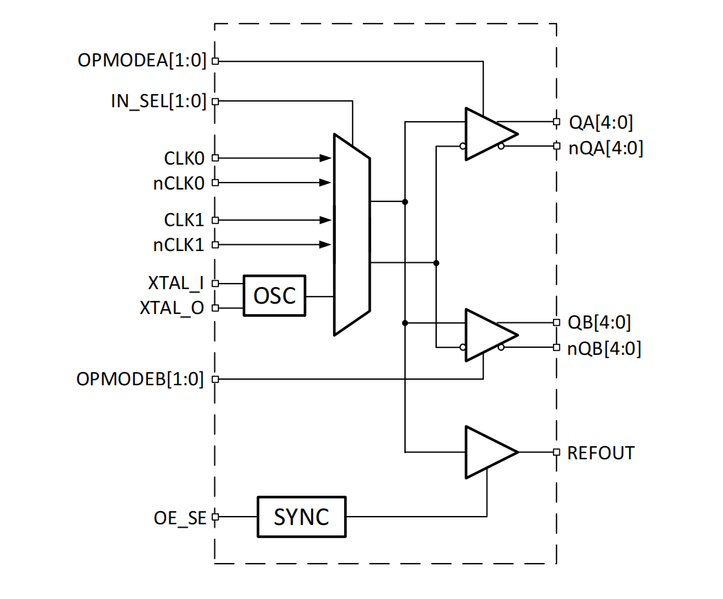
• Two differential reference clock pairs
• Input pairs can accept the following
differential input levels: LVPECL, LVDS,
HCSL, HSTL or Single Ended
• Crystal Input accepts 10MHz to 100MHz
Crystal or Single Ended Clock
• Maximum Output Frequency
LVPECL - 2GHz
LVDS - 2GHz
HCSL - 350MHz
LVCMOS - 250MHz
• Two banks, each has five differential
output pairs that can be separately
configured as LVPECL or LVDS or HCSL
or Hi-Z
• One single-ended reference output with
synchronous enable to avoid glitch
• Output skew: 30ps (typical)
• Part-to-part skew: 60ps (typical)
• Additive RMS phase jitter @ 156.25MHz:
50 fs RMS (10kHz - 20MHz), @
3.3V/ 3.3V
• Supply voltage modes:
VDD VDDO
3.3V 3.3V
3.3V 2.5V
2.5V 2.5V
• Industrial Temperature Range: -40°C to 85°C
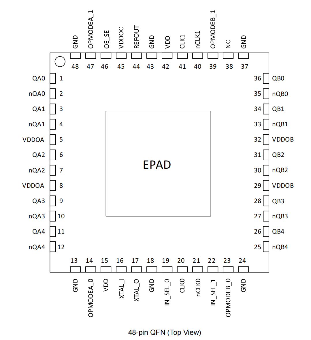
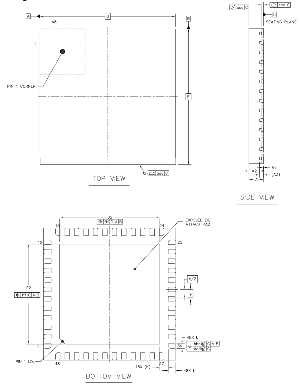
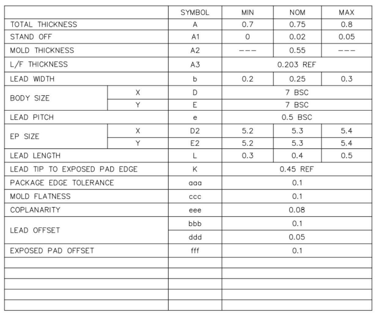
• Available in 48-pin, 7mm*7mm QFN package


