POP_UP_MESSAGE_CONTENT


Wet and dry etching of semiconductors
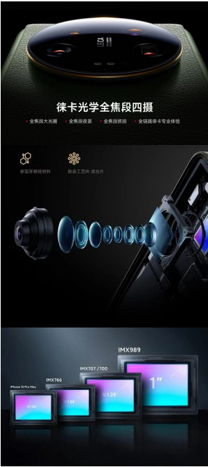
So how does the Leica camera of Xiaomi 13 Ultra capture images? The mobile phone camera chip will segment the captured scene, such as a landscape painting. After segmentation, the result is as follows:
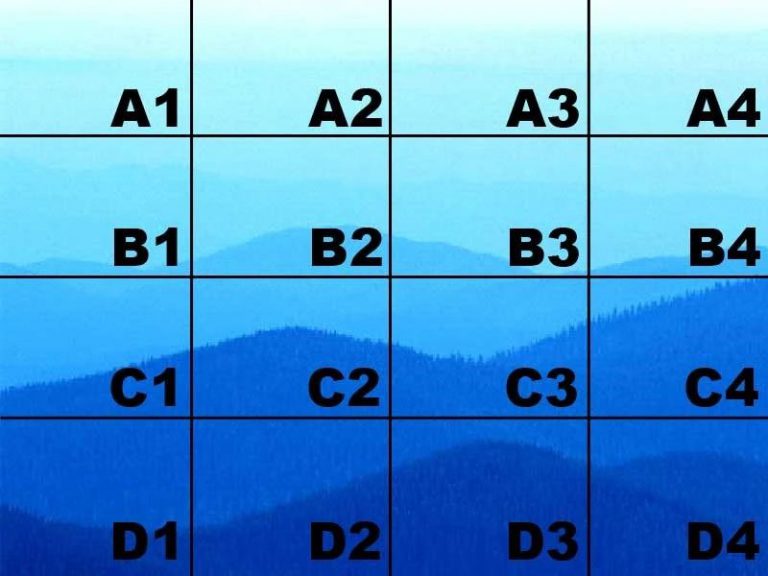
The pixels of the camera are calculated based on the number of segmented units. The image above has 4 pixels horizontally and 4 pixels vertically, multiplied by 16, resulting in a 16 pixel image. If you want to see a picture clearly enough, you need to divide the picture into smaller cells. If the horizontal axis is divided into 1000 pixels and the vertical axis is also divided into 1000 pixels, then it is a million pixel camera. The method of dividing the camera chip into small cells is etching. The following is a partial detail image of a semiconductor chip after etching is completed:
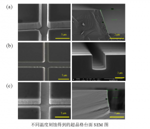
The microstructure after semiconductor etching is somewhat similar to farmland in the south, where a large area of farmland is processed into neat ditches using agricultural machinery. The farmland is divided into square units, and rice or wheat is planted on the unit farmland.
Semiconductor etching method
Etching can be divided into two types: wet etching and dry etching. For ease of understanding, let me give another example.
When we take a shower, there are two ways of bathing. One is the northern bathing method, where we put a pool of water in the bathhouse, soak in it, and start scrubbing. We are exposed to bath water all over our bodies, which is called wet method. Because water comes into contact in various places without discrimination, the term is called isotropic.
Another method is the Southern Cleansing Method, where a small room is equipped with a nozzle and you can spray your arms and thighs if you want to wash them, precisely controlling the cleaning area. This method is called the Dry Method. Not every place comes into contact with water, this is called anisotropy.
In addition, when we have a wound on our arm, we don't want the wound to come into contact with water when taking a shower. We can choose to stick waterproof patches on the wound to prevent the area from getting wet. Before semiconductor etching, some areas are also chosen not to be etched. The method used is to apply photoresist to protect the semiconductor surface, which is why lithography and etching often occur simultaneously.
What is wet etching?
Wet corrosion is an indispensable process technology in the production of compound semiconductor devices. The main principle is that the corrosion solution reacts chemically with the material immersed in the corrosion solution to generate soluble products, thereby removing the area that needs to be corroded.
It generally corrodes the material under the protection of photoresist, cleans and removes the photoresist to obtain the final pattern. When corroding semiconductor wafer materials such as silicon or silicon oxide, HNO3 or HF is usually chosen, and the reaction equation is as follows:
Si + 4HNO3 → SiO2 + 2H2O + 4NO2.SiO2+ 6HF → H2SiF6 +2H2O.
That is to say, immerse the wafer in HNO3 or HF and let the strong acid remove a certain part of the wafer. The wet etching process is simple, economical, mature and universal in photolithography mask preparation technology, and the selection of photoresist in the etching solution is generally high, which is conducive to selective etching. The corrosion rate is determined by the activity of the corrosive agent and the solubility and diffusion of the corrosion products.
However, wet corrosion has natural corrosion isotropy, and the downward cutting under the mask makes it unsuitable for making patterns smaller than 2 microns. During the wet corrosion process, bubbles will also form, and the areas where bubbles adhere will cause corrosion to terminate. In addition, wet corrosion also has some other issues, such as safety hazards caused by exposure to chemicals and generated gases, as well as environmental hazards caused by chemical emissions requiring waste treatment.
What is dry etching?
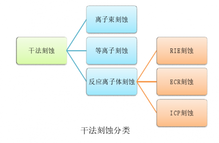
Compared to wet etching, dry etching has more obvious advantages. Dry etching has anisotropy and can fundamentally improve problems such as lateral drilling. Dry etching can be divided into three types: physical etching, chemical etching, and physicochemical etching.
The following are several commonly used etching techniques for industrial preparation, including Ion Beam Etching (IBE), Reactive Ion Etching (RIE), and later Electron Cyclotron Resonance (ECR) and Inductively Coupled Plasma (ICP) based on high-density plasma reactive ions.
What is plasma?
Plasma is an ionized gas with roughly equal densities of positive ions and electrons, composed of ions, electrons, free radicals, photons, and neutral particles, and is the fourth state of matter. For example, we all know that atoms are composed of atomic nuclei and outer electrons, similar to the walnuts we buy, which have walnuts and outer shells. Under normal circumstances, the shell is wrapped in walnuts. Apply an external force to the walnut to separate it from the shell. The walnut is positively charged, while the shell is negatively charged. A pile of material composed of many walnuts and walnut shells is called a plasma walnut.

(1) IBE dry etching:
IBE, also known as ion milling, is a pure physical etching technique developed in the 1970s. Its principle is to use an ion beam generated by an inert gas (such as Ar, Xe, etc.) to rapidly bombard the surface of a target material under the action of an accelerating voltage. During the bombardment process, the ion beam continuously transfers energy to the surface atoms of the material. When the accumulated energy of the surface atoms exceeds their own binding energy, they will detach from the solid surface and undergo sputtering, thereby achieving the purpose of etching. The schematic diagram of its principle is shown in the following figure.
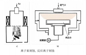
This technology uses acceleration voltage to control the direction and energy of the ion beam, resulting in excellent anisotropy and rate controllability in etching. In addition, it belongs to pure physical etching and can be applied to a wide range of materials. It still plays an important role in etching materials with very stable chemical properties, such as ceramics and certain metals. But precisely because of this, the mask selection ratio of this technology is often low, and a thick mask is required when etching deeper grooves, which affects the etching accuracy; Moreover, high-speed ion beams can easily cause surface lattice damage, leading to inevitable electrical damage to the device.
(2) RIE dry etching:
RIE is a dry etching technique developed on the basis of IBE, which is mainly based on chemical reactions and supplemented by ion physical bombardment. Compared with IBE, RIE has a higher etching rate and also exhibits excellent anisotropy and large-area uniformity, making it one of the most widely used etching techniques in micro nano processing. The schematic diagram of its structure is shown in the following figure. When radio frequency voltage is applied on both sides of the parallel plate electrode system, the electrons in the chamber will accelerate and bombard the reaction gas, causing ionization. During the ionization process, free electrons will be further generated to continue to participate in collisions until an equilibrium glow discharge state is reached, forming a stable plasma on one side of the parallel plate.
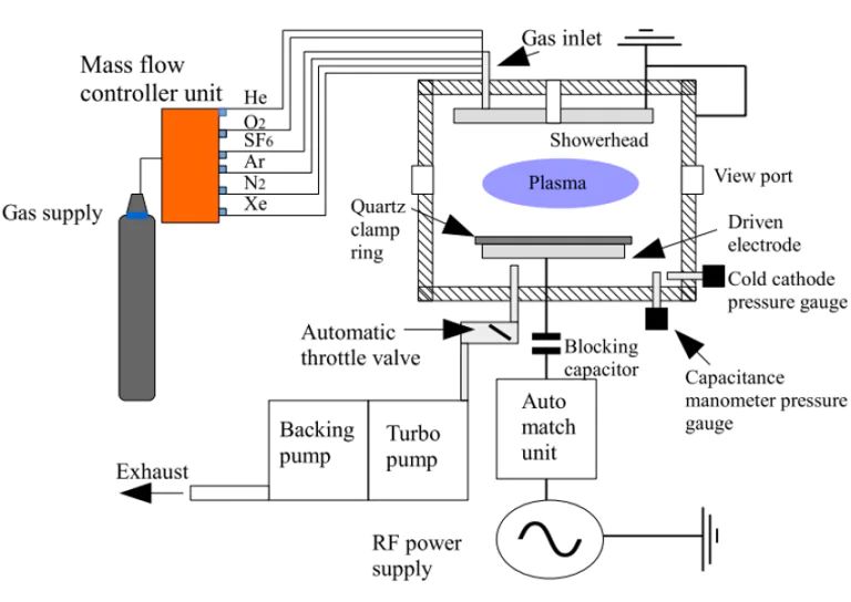
Generally speaking, RIE etching requires reaction products to have a certain degree of volatility in order to be effectively and timely evacuated by the vacuum system during the etching process, thereby avoiding secondary deposition and maintaining high etching accuracy. In the RIE etching system, the RF power of the RF electric field directly determines the concentration of the plasma and the magnitude of the acceleration bias voltage, which can then control the etching rate. Unfortunately, RIE increases the plasma density while also increasing the acceleration bias voltage, which accelerates the bombardment of ions and gives them higher energy. This may cause lattice damage to the material and reduce the mask selectivity ratio. Therefore, it still has certain limitations in etching applications. With the rapid development of large-scale integrated circuits, the size of transistors continues to shrink, which puts higher demands on the accuracy, aspect ratio, and other indicators of micro nano processing technology. Therefore, dry etching technology based on high-density plasma has emerged, bringing new hope for the further development of electronic information technology.
(3) ECR dry etching:
One early way to achieve high-density plasma was based on microwave electron cyclotron resonance technology, namely ECR etching technology. The schematic diagram of its structure is shown below.
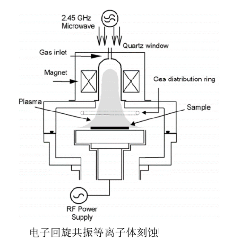
The system imports high-frequency microwaves (~2.5GHz) from the top, uses the microwaves to resonate with electrons inside the cavity, and applies a uniformly distributed magnetic field outside the cavity that matches its frequency, causing electrons to undergo cyclotron resonance to obtain higher energy and thus improve ionization rate. By using this method, plasma densities higher than 10E11/cm3 can be obtained, which is at least two orders of magnitude higher than RIE (10E9-10E10/cm3). Meanwhile, the bottom sample stage is still connected to the RF source, and the acceleration bias voltage of the plasma can be independently controlled by controlling the power of the RF source. The emergence of ECR etching technology has compensated for the disadvantage of RIE etching technology that cannot control plasma density and bias voltage separately. At the same time, high-density plasma greatly improves the etching rate and mask selection ratio, promoting the realization of ultra-high aspect ratio etching patterns in micro nano processing. However, the implementation of this technology relies on the joint action of multiple systems such as microwave sources, radio frequency sources, and magnetic fields. The device structure design is generally complex, and there are also issues of mutual adjustment and matching between various radio frequency sources, which brings certain difficulties to practical operation. Therefore, shortly after the proposal of ECR etching technology, a new ICP etching technology was derived.
(4) ICP dry etching:
ICP etching technology is further simplified based on ECR technology. Two 13.56MHz RF sources are used to control the generation of plasma and the magnitude of acceleration bias voltage, respectively. At the same time, an alternating electromagnetic field is induced by a spiral coil to replace the external magnetic field in ECR. The schematic diagram of its structure is shown below. The RF source transfers energy to the internal electrons through electromagnetic coupling, and the electrons undergo cyclotron motion and collide with the reaction gas in the induced electromagnetic field to ionize them, and can obtain a plasma density equivalent to ECR. ICP etching technology basically combines all the advantages of the above-mentioned etching systems, while meeting the requirements of high etching rate, high selectivity, large-area uniformity, and simple and easy to control equipment structure. Therefore, it has quickly replaced ECR as the first choice for the new generation of high-density plasma etching technology.

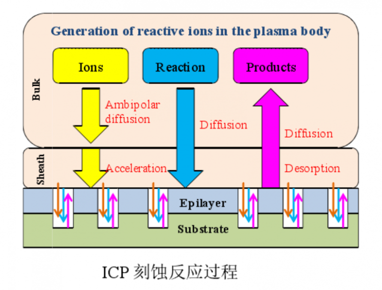
The following is a schematic diagram of the ICP etching reaction process. Glow discharge generates active ions, which then undergo chemical reactions with the sample. Physical active ions assist in breaking chemical bonds, accelerating reactant desorption, promoting surface chemical reactions, and removing non-volatile residues on the surface. The physical and chemical processes together constitute the three stages in the etching process.
6、 Common problems in dry etching
There are various factors that affect the results of dry etching, with the most common being load effect, trench effect, and charging effect.
(1) Load effect:
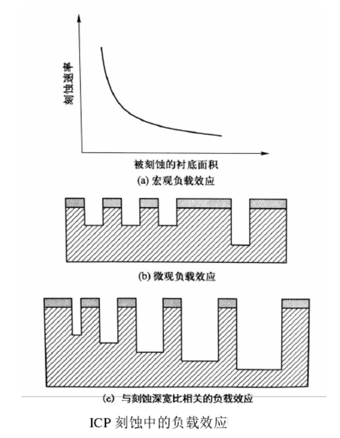
Loading effect is one of the most common problems in etching, which mainly refers to the effect of reduced etching rate or uneven etching caused by insufficient reactive plasma during the etching process. There are various reasons that can cause load effects, and according to different reasons, this effect can be further divided into macro load effects and micro load effects, as shown in the following figure. The load effect is determined by the characteristics of the etching system and is commonly present in all reactive ion etching. In order to alleviate the impact of this effect on the etching results, on the one hand, a higher density and more evenly distributed plasma is required. On the other hand, auxiliary gases can be added to the reaction gas to dilute and homogenize the plasma, improve the performance of the vacuum system to accelerate the exchange of plasma and the extraction of etching products, and pay attention to balancing the density of patterns when designing photolithography plates.
(2) Microgroove effect
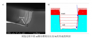
The Trenching effect refers to the phenomenon of chamfering caused by the etching rate near the sidewall being greater than the etching rate at the center of the trench during the etching process, as shown in the following figure. This effect is caused by high-energy particles hitting the etched sidewall at a certain angle, but the energy is not completely lost and is reflected by the sidewall, sliding down to the bottom to continue etching. The occurrence of this effect is related to the incident angle of high-energy particles and the inclination angle of the sidewall. Therefore, the appearance of sidewall grooves is often accompanied by non completely steep sidewalls. Figure B shows the Monte Carlo simulation verification of this effect, where the groove effect at the corners becomes more pronounced as the etching depth increases. Increasing RF power can to some extent enhance the collimation of incident particles, thereby improving sidewall steepness and reducing groove effects. However, in addition, the accumulation of negative charges from etching the mask will also to some extent exacerbate the generation of sidewall grooves, as explained in the charging effect later.
(3) Charging effect
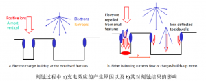
The charging effect is caused by the insulation of the etching mask. The reactive plasma is an equilibrium state of positively charged ions and negatively charged electrons. Under the action of bias voltage, the reactive ions are vertically incident on the etching surface. However, due to the light weight and fast speed of electrons, they have a certain degree of anisotropy. Some electrons that overcome the reverse potential and reach the surface of the sample gather on the non-conductive mask surface, forming a micro localized electric field at the top of the sample, which has a certain influence on the direction of the incident particles, as shown in Figure a). On the one hand, positively charged reactive ions will deflect under the action of this electric field and bombard the etched sidewalls, resulting in a decrease in the anisotropy of etching, as shown in Figure b); On the other hand, this electric field can also exacerbate the groove effect by affecting the incident angle of charged particles. This effect is more common in etching narrow channel patterns, and the longer the etching time, the more electrons accumulate, making this effect more pronounced. This effect can be mitigated by using appropriate etching masks or intermittent etching.
