POP_UP_MESSAGE_CONTENT


Why are wafers round? Is the chip square?
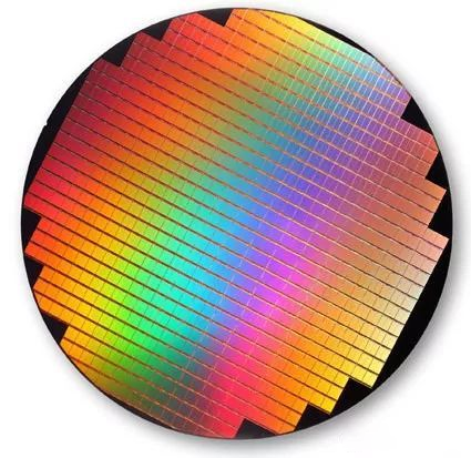
Because the manufacturing process determines that it is circular. The purified high-purity polycrystalline silicon is grown by rotating on a seed. After the polycrystalline silicon is melted, it is placed in a quartz crucible. Then, the sub crystals are placed in the crucible and rotated uniformly while being pulled upwards. The melted silicon will form a cylindrical ingot along the sub crystal direction.
This method is the CZ method (Czochralski) that has been used all along, also known as single crystal Czochralski method. As shown in the following figure:

Then the silicon ingot is cut into silicon wafers through diamond wire cutting:
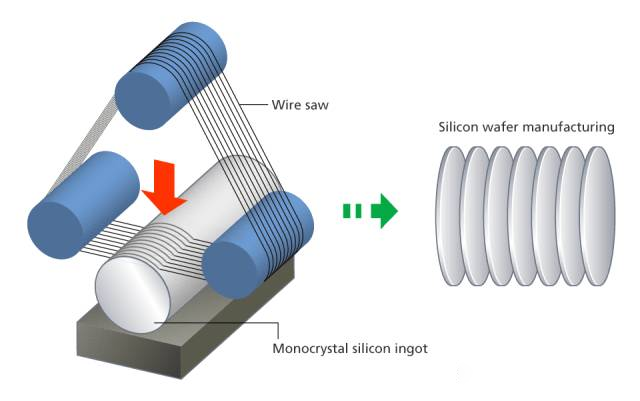
After polishing and other treatments, the silicon wafer can proceed with subsequent processes.
The rotational pulling in the single crystal pulling process determines the cylindrical shape of the silicon ingot, which in turn determines the circular shape of the wafer.
The process of the Czochralski method is to first heat high-purity silicon into a molten state in a crucible, then place the seed crystal at the end of a precisely oriented rod and immerse the end into the molten silicon, and then slowly pull and rotate the rod upwards.
By precisely controlling the pulling rate, rotation rate, and temperature, a larger cylindrical monocrystalline silicon rod can be obtained at the end of the rod. After subsequent polishing, cutting, and other processes, a usable circular silicon wafer can be obtained. So, the roundness of the wafer is due to the "roundness" of the silicon rod. However, to be precise, the wafer is not completely circular.
Why wasn't it round again later? In fact, there is a process that has been skipped in the middle, which is Flat/Notch Grinning.

Usually, a notch is ground around the silicon wafer after it is processed into a wafer.
Cutting a flat corner on silicon ingots below 200mm is called Flat.
On silicon ingots above 200mm (inclusive), in order to reduce waste, only a small circular opening is cut, called Notch. After slicing, the wafer becomes like this:
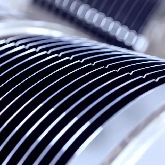
If you carefully look at the first image of this article, you will find that it actually has a small gap missing.
Why do we have to do this? In fact, this small gap is destined to be useless in the production of Die because it is too close to the edge and very small. This can help determine the placement of the wafer in subsequent processes, and for positioning, the crystal orientation of the single crystal growth is also indicated.
The positioning device can be as follows:
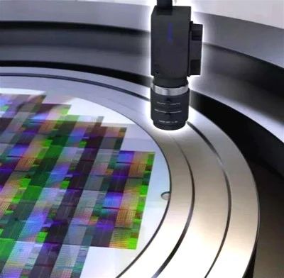
This makes cutting and testing more convenient. Strictly speaking, all wafers are not circular. If we ignore the small issues of Flat/Notch, its circular shape is determined by the process.
Circular chips are actually more difficult to manufacture
After undergoing steps such as coating, photolithography, etching, and ion implantation, silicon wafers are manufactured one by one. However, at this time, the chips are still "grown" on the wafer and need to be cut to become individual chips.
Imagine that a square chip can be completely cut off with just a few cuts. What if it's a circular chip? I'm afraid it will take several times more time to cut than a square. From the perspective of packaging, square shaped chips are also convenient for lead operation. Even for Flip chip type packaging, square shaped chips are more convenient for machine operation to align I/O interfaces with solder pads.
The most important point is that circular chips cannot solve the problem of wasted silicon wafer area. Cut many square areas on a wafer without gaps in between, leaving only empty spaces at the edges of the wafer. But if many circular areas are cut from a plane, there will definitely be some wasted areas in the middle, and waste on the periphery of the wafer cannot be avoided.

Actually, saving wafer area has always been an important issue. The more chips that can be produced on a wafer, the higher the production efficiency and the lower the cost of a single chip. The best way to solve production efficiency at present is to increase the wafer area.
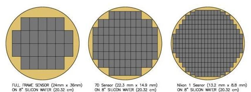
From the picture, it can be simply seen that when the chip area is fixed, using larger wafers can effectively improve wafer utilization. According to the calculation formula commonly used by Fab factories internationally:

Producing 100mm ² chips on a 12 inch wafer can produce approximately 660 chips, while using an 8-inch wafer only yields 180 chips, reducing the wafer area by 50% but reducing the number of chips by 72%.
Therefore, currently 12 inch wafers have become the main battlefield for larger IDM and foundry manufacturers worldwide. At present, only a small number of enterprises in our country have the manufacturing technology of 12 inch semiconductor silicon wafers, and domestic enterprises are accelerating to catch up with the world's leading companies.
Finally, to summarize the question raised in the title, why is the chip square? Circular chips are difficult to cut, and the subsequent packaging stage is also inconvenient to control. Most importantly, circular chips cannot solve the problem of wasted wafer area. Why are wafers round? In the process of producing chips, circular wafers are more convenient to produce and have higher yield due to mechanical factors, and the silicon rods are naturally cylindrical, so the wafers are naturally circular.
Disclaimer: The article is sourced from the official account of the Institute of Semiconductors, Chinese Academy of Sciences. It is reproduced for the purpose of transmitting more information, only for sharing and learning, not for any commercial purpose, and does not represent the company's view. If it involves the content, copyright and other issues of the work, please contact us for deletion.


