POP_UP_MESSAGE_CONTENT


Wet etching and dry etching in chip manufacturing
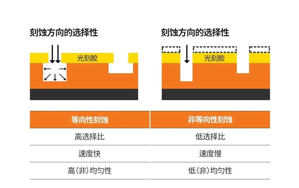
The first key term is' selection ratio '. This parameter is used to measure the difference in etching rate between target and non target materials during the etching process. The larger the selection ratio, the greater the difference in etching rate. In the etching reaction process shown in the above figure, a portion of the photoresist mask will also be etched. Therefore, in the actual etching process, it is impossible to achieve the effect of only etching and removing the target material 100%. A set of high selectivity etching process parameters can efficiently remove the etching target material while retaining as much non etching target material as possible.
The second keyword is' directional selectivity '. As the name suggests, directional selectivity refers to the direction of etching. This property can be divided into two types: isotropic and anisotropic etching: isotropic etching has no directional selectivity, and in addition to longitudinal reactions, lateral reactions also occur simultaneously; Non isotropic etching refers to the use of directional ion impacts to etch in a specific direction, forming a vertical contour. Imagine a candy packaging bag leaking a hole. If the entire candy is placed in water along with the packaging bag, after a period of time, the candy will dissolve. But if only the laser is irradiated towards the opening, the candy will be burned through, forming a hole instead of the entire candy being burned away. The former phenomenon is like isotropic etching, while the latter phenomenon is like anisotropic etching.
The third keyword is' Etching Rate ', which indicates the speed of etching. If other parameters remain unchanged, of course, the faster the speed, the better, but generally there is no perfect choice that is both fast and accurate. In the process of process research and development, it is often necessary to balance parameters such as accuracy with rate. For example, in order to improve the non isotropy of etching, it is necessary to reduce the pressure of the etching gas, but reducing the pressure means that the amount of gas that can participate in the reaction decreases, which naturally slows down the etching rate.
The last keyword is' uniformity '. Uniformity is a parameter that measures the etching ability of the etching process on the entire wafer, reflecting the degree of non-uniformity in etching. Etching is different from exposure, as it requires exposing the entire wafer to etching gas. In this process, the by-products are removed after the reaction gas is applied, and the substances need to be recycled continuously, so it is difficult to make every corner of the entire wafer identical. This results in different etching rates in different parts of the wafer.
Why etch?
There are many uses for chip etching. Initially, the wafer was a silicon wafer without any function. How to transform this flat plate into the required structure? This requires microfabrication of the wafer. The following is a partial detail image of a semiconductor chip after etching is completed:
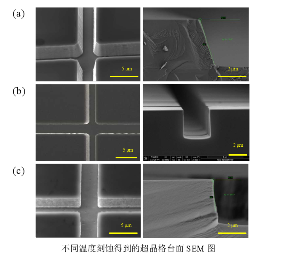
The etched microstructure is somewhat similar to farmland in the south, where a large area of farmland is processed into neat channels using agricultural machinery. The farmland is divided into square units, and rice or wheat is planted on each unit of farmland.
Types of Etching: Wet Etching and Dry Etching
Etching, like oxidation process, is divided into wet etching and dry etching.
Wet Etching
It is a pure chemical reaction that uses chemical reagents to react with the etched material to produce soluble or volatile substances. The selected etching solution should have the ability to uniformly remove the surface layer of the wafer without damaging the next layer of material.
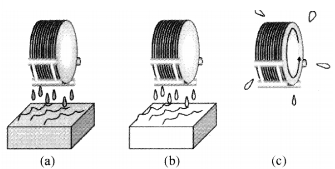
Process flow: The groove etching system immerses the wafer in an etching solution, and after a certain period of time, it is transferred to the cleaning equipment to remove residual pollutants, and then sent to the final cleaning station for rinsing and spin drying.
When corroding wafer materials such as silicon or silicon oxide, HNO3 or HF is usually chosen, and the reaction equation is as follows:

That is to say, immerse the wafer in HNO3 or HF and let the strong acid remove the material in contact with the etching liquid.
The wet etching process is simple, economical, mature and universal in photolithography mask preparation technology, and the selection of photoresist in the etching solution is generally high, which is conducive to selective etching. The corrosion rate is determined by the activity of the corrosive agent and the solubility and diffusion of the corrosion products. However, wet corrosion has natural corrosion isotropy, and the downward cutting under the mask makes it unsuitable for making patterns smaller than 2 microns. During the wet corrosion process, bubbles will also form, and the areas where bubbles adhere will cause corrosion to terminate.
In addition, wet corrosion also has some other issues, such as safety hazards caused by exposure to chemicals and generated gases, as well as environmental hazards caused by chemical emissions requiring waste treatment.
Dry Etching
The method of using plasma activated chemical reactions or high-energy ion beam bombardment to remove substances. The etching method using gas as the main medium does not require liquid chemicals or rinsing on the wafer, hence it is called dry etching. The three dry etching techniques are plasma etching, ion milling etching, and reactive ion etching.
Plasma etching: a technique of thin film etching using plasma, which uses etching gas to form active groups in the plasma under the acceleration of an electric field, and undergoes chemical reactions with the etched material to form by-products that are carried away by the gas flow.
Ion milling etching: It is a pure physical etching technology developed in the 1970s. Its principle is to use an ion beam generated by inert gases (such as Ar, Xe, etc.) to rapidly bombard the surface of the target material under the action of an accelerating voltage. During the bombardment process, the ion beam continuously transfers energy to the surface atoms of the material. When the accumulated energy of the surface atoms is greater than their own binding energy, they will detach from the solid surface and undergo sputtering, thereby achieving the purpose of etching. The schematic diagram of its principle is shown in the following figure.
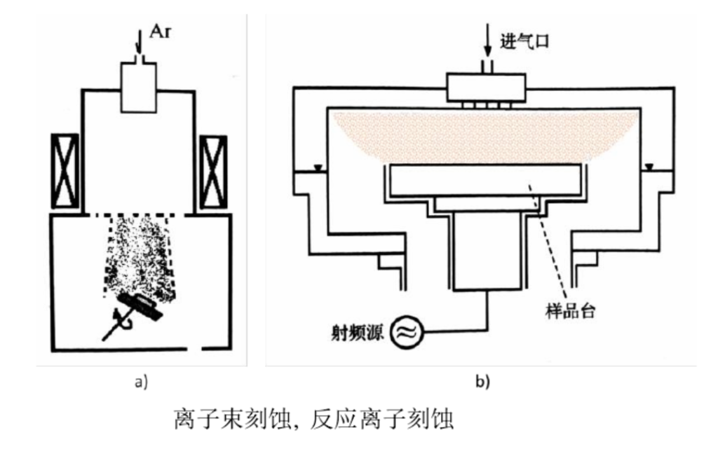
This technology uses acceleration voltage to control the direction and energy of the ion beam, resulting in excellent anisotropy and rate controllability in etching. In addition, it belongs to pure physical etching and can be applied to a wide range of materials. It still plays an important role in etching materials with very stable chemical properties, such as ceramics and certain metals.
But precisely because of this, the mask selection ratio of this technology is often low, and a thick mask is required when etching deeper grooves, which affects the etching accuracy; Moreover, high-speed ion beams can easily cause surface lattice damage, leading to inevitable electrical damage to the device.
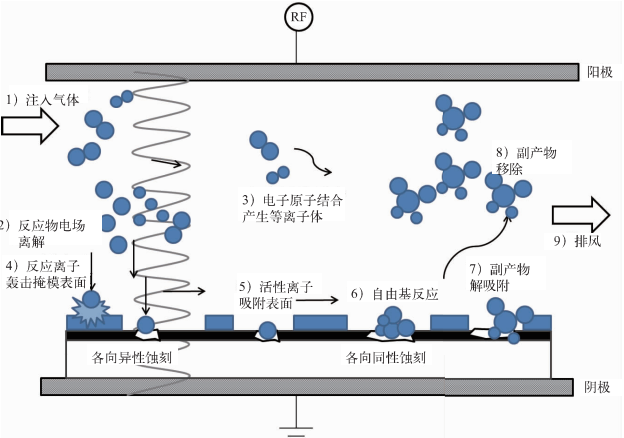
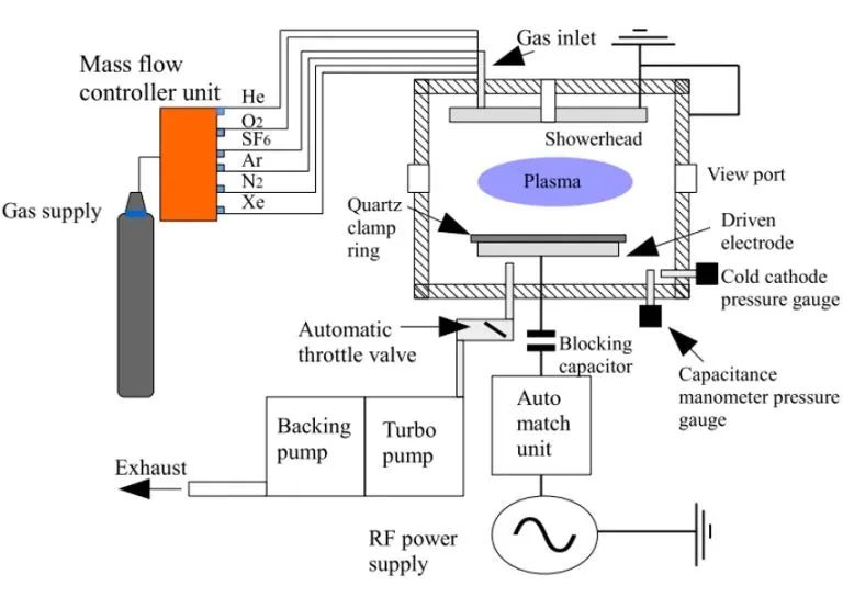
Reactive ion etching: Combining the principles of plasma etching and ion milling etching, it has a higher etching rate and also exhibits excellent anisotropy and large-area uniformity. It is currently one of the most widely used etching techniques in micro nano processing. The schematic diagram of its structure is shown in the following figure. When radio frequency voltage is applied on both sides of the parallel plate electrode system, the electrons in the chamber will accelerate and bombard the reaction gas, causing ionization. During the ionization process, free electrons will be further generated to continue to participate in collisions until an equilibrium glow discharge state is reached, forming a stable plasma on one side of the parallel plate.
How to choose etching process?
Firstly, according to the process requirements of the chip product, if only dry etching is capable of performing the etching task, dry etching should be selected; If both dry and wet etching methods are capable, wet etching is generally chosen because it is more economical; If you want to precisely control the line width or the vertical/conical angle of engraving, then choose the dry method.

Of course, there are also some special structures that require wet etching. For example, the inverted pyramid structure of silicon etching in MEMS can only be achieved through wet etching.


